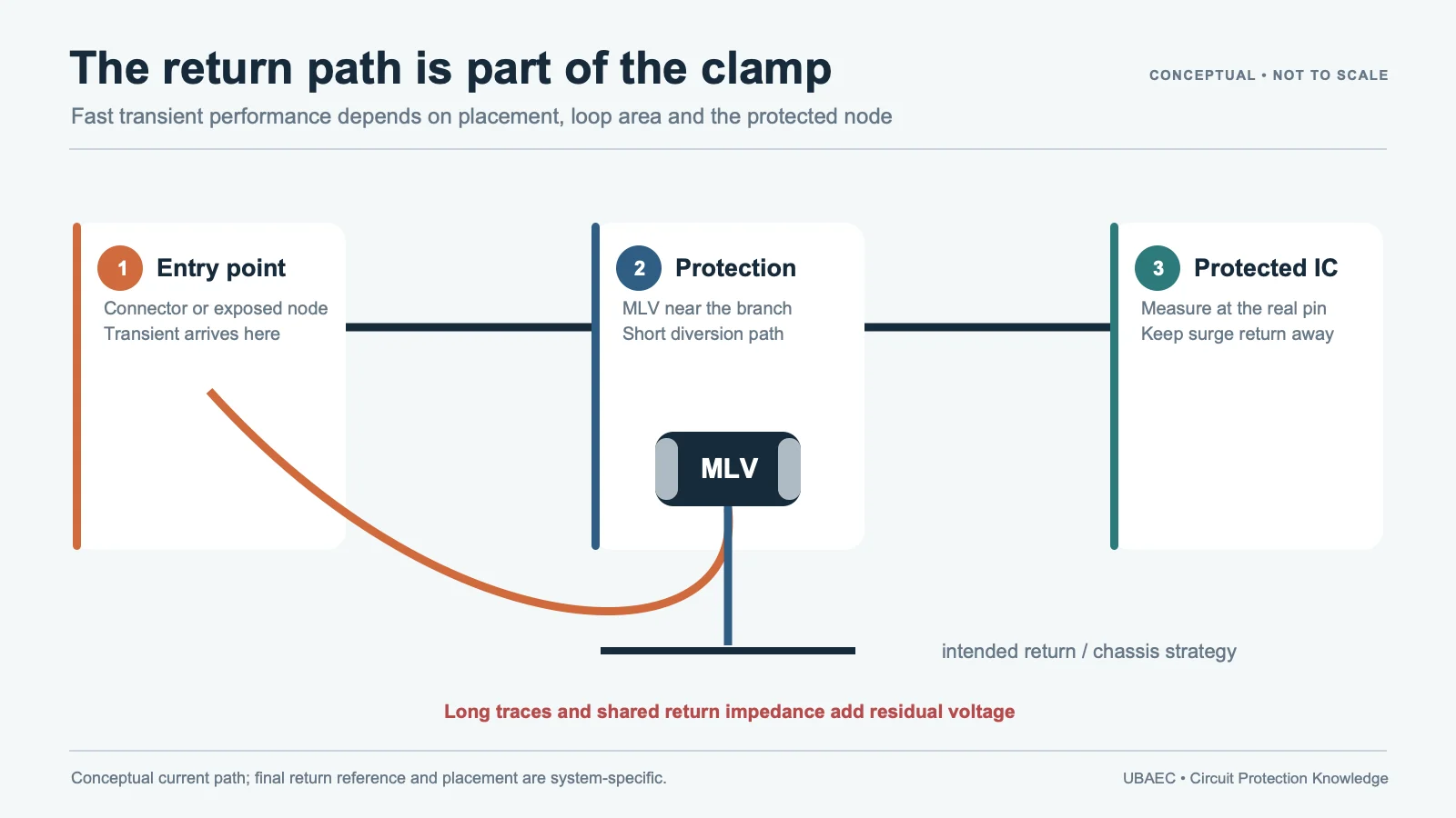
The measured curve of a multilayer varistor (MLV) is only one part of protection performance. The printed circuit board (PCB) decides how much transient current reaches the device, where that current returns and how much extra voltage is created by interconnect inductance. The assembly process also decides whether the ceramic body and terminations remain intact.
Place the MLV at the Exposure Point
For connector or exposed-node protection, place the shunt device close to the entry point so the transient encounters the protection path before long protected-side routing. Avoid a long branch that lets current pass the protected circuit and return to the MLV later. Manufacturer demonstrations of PCB layout for electrostatic-discharge countermeasures illustrate why the current path can change the measured result.
Keep the Diversion Loop Short
Fast current change through trace and via inductance produces additional voltage. Minimize the loop from entry point through the MLV to the intended return. Use an appropriate return plane or node for the system architecture; “ground” is not automatically the same low-impedance return at transient frequencies.
Separate Dirty and Protected Routing
Avoid close parallel routing that recouples the transient around the protector. Keep the protected-side trace away from the incoming path where practical, and coordinate connector shield, chassis, signal reference and circuit ground deliberately.
Use the Exact Land Pattern
Pad geometry and solder volume affect termination stress and board strain. Use the land pattern for the exact package, termination and revision. Do not publish one universal pad dimension or assume that two equal-size MLVs share the same recommended footprint.
Control Soldering Heat
Follow the supplier’s preheat, ramp, peak, time, alloy, cycle-count and cooling guidance. Excessive peak/time, rapid temperature change, repeated reflow or an unsuitable flow process can damage the ceramic, termination or solder joint. Profile the real board because thermal mass changes the component’s exposure.
Manage PCB Flex and Depanelization
Board bending can crack a ceramic chip or damage a termination. Risk increases near board edges, score lines, connectors, screws and areas that flex during insertion or depanelization. Review package orientation relative to the principal bending direction, support the PCB and choose a low-strain separation method. Also account for coefficient-of-thermal-expansion (CTE) mismatch where temperature cycling is significant.
No universal safe distance or bend value applies. Use the exact manufacturer guidance and validate the mounted assembly.
Cleaning, Contamination and Coating
Flux residue, ionic contamination, incompatible cleaning and trapped moisture can affect surface leakage or corrosion. Follow supplier material-compatibility guidance. Conformal coating does not repair a cracked component or prove high-humidity qualification.
Inspection and Post-Process Checks
- verify component identity, orientation where topology matters and placement;
- inspect solder fillet, wetting, bridging, insufficient/excess solder and body damage;
- review depanelization and connector/screw loads;
- measure relevant electrical fields after the full assembly sequence;
- use microscopy or other appropriate analysis when latent cracking is suspected.
Validate Electrical and Mechanical Performance Together
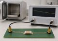
A board may have an intact solder joint yet still provide a poor transient return path; it may also show good clamp results before mechanical damage creates leakage or intermittent behavior. Validate placement/current path with oscilloscope and equipment-level tests, then check electrical drift and physical condition after assembly and representative mechanical/environmental stress.
Use MLV reliability, standards and failure modes for evidence layers, How to Select an MLV for the full workflow and the UBAEC Applications section for interface-specific topology.
Layout and Assembly Checklist
- Locate the transient entry and intended return.
- Place the MLV before protected-side routing.
- Minimize trace/via loop inductance and recoupling.
- Use exact package land and solder guidance.
- Profile the real reflow/flow process and cycle count.
- Reduce board flex during assembly, use and depanelization.
- Inspect and electrically measure after processing.
- Run the final PCB/system transient test and retain results.
Summary
MLV layout is both an electrical-current-path problem and a ceramic-assembly problem. Short diversion paths improve clamping; correct land, solder and strain controls protect the component. Exact dimensions and profiles always come from the selected series.
Continue Reading
- How Multilayer Varistors Work
- How to Select an MLV
- MLV Reliability, Standards and Failure Modes
- MLV Knowledge Map
Official Technical References
The following first-party, standards-organization or publisher records support the technical boundaries used in this article. Always verify the current revision and the exact product scope before design release.
- The Key to Successful ESD Protection: GND Pattern Design and Use of ESD Protection Components
- Safety precautions for chip-type multilayer varistors
- Precautions for Varistors
- PCB Layout for ESD Countermeasures: ESD Visualization
- Safety precautions for automotive-grade multilayer varistors
- Design Support Data List