
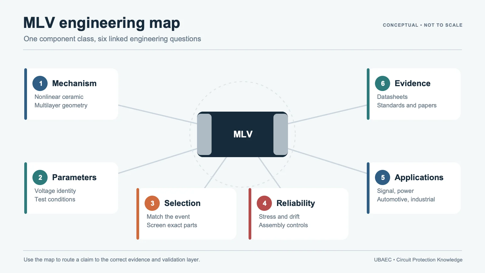

MLV means multilayer varistor, also called a multilayer chip varistor. It is a voltage-dependent ceramic component used near sensitive circuits to limit electrostatic discharge (ESD) and other transient overvoltage events. Whether an MLV is suitable depends on the exact device, circuit, transient test, layout and required system performance.
This Knowledge Map gives you the minimum information needed to understand the component class, read its datasheet, build a shortlist and plan validation. Deeper definitions belong in the MLV Wiki, while interface-specific protection and testing belong in Applications.
Explore the MLV Knowledge Map
Choose a path by engineering task. Each guide keeps general principles separate from exact series data, test conditions and final-system validation.
Start with the Fundamentals
Definitions, operating mechanism and the boundary between general MLV knowledge and product-specific evidence.
- MLV Terminology and Product Boundaries — Learn how MLV, MLCV, chip varistor, SMD MOV and ESD suppressor terms differ by construction, package, topology and application role.
- How Multilayer Varistors Work — See how grain-boundary nonlinearity and multilayer electrode geometry allow an MLV to divert transient current and limit voltage.
- MLV Materials, Microstructure and Manufacturing Overview — Learn the general material, microstructure and process stages behind multilayer varistors without confusing research or patents with a commercial production recipe.
Read, Select and Validate
Parameter identity, test conditions, selection workflow, reliability, layout and frequently asked engineering questions.
- MLV Datasheet Parameters and Test Conditions — Learn how to read MLV datasheet fields without mixing working voltage, varistor voltage, clamping voltage or mismatched pulse and capacitance conditions.
- How to Select an MLV: A Practical Engineering Workflow — Follow a condition-based workflow from circuit voltage and transient source to MLV screening, layout, evidence review and final system validation.
- MLV Reliability, Standards and Failure Modes — Separate datasheet limits, qualification, pulse ageing, environmental stress and final-system immunity when reviewing MLV reliability and failure modes.
- MLV PCB Layout, Mounting and Soldering Reliability — Improve MLV protection with short current paths, correct placement, series-specific footprints, controlled soldering and board-flex risk management.
- MLV Technical FAQ: Parameters, Selection and Reliability — Find short answers on MLV meaning, voltage fields, waveforms, capacitance, selection, qualification, layout and reliability, with links to full guides.
- MLV Technical Resources & Datasheet Library — Browse curated MLV technical resources with source owner, document scope, version or lifecycle context, evidence boundary and review status.
Compare Technologies and Research Product Families
Technology comparisons, array topologies, manufacturer-source research and evidence-controlled cross-referencing.
- MLV vs TVS Diode: How to Compare Protection Devices — Compare MLVs and TVS diodes by construction, voltage fields, clamp test, capacitance, leakage, pulse duty, package, temperature and validation—not by a universal winner claim.
- MLV vs SMD MOV and Disc MOV — SMD describes mounting and MOV describes a material family. Learn why ceramic MLV, molded SMD MOV and disc MOV ratings must remain construction- and condition-specific.
- MLV vs Resin and Polymer ESD Suppressors — Similar chip and ESD labels can hide different ceramic, resin/thick-film and polymer constructions. Compare exact parts by evidence and matched conditions.
- MLV Arrays, Multi-Element Devices and Feedthrough Filters — Learn how discrete MLVs, arrays, shared-terminal devices, differential 2-in-1 parts and feedthrough filters differ in topology, ratings and validation.
- MLV Manufacturer and Product-Family Research Map — Explore a dated, non-ranking map of MLV manufacturers and families using current, conditional and historical first-party evidence labels.
- How to Cross-Reference MLVs Safely — Cross-reference MLVs by exact construction, topology, package, voltage definitions, waveform, capacitance, qualification, lifecycle and final-system testing.
Consumer and High-Speed Interfaces
Protection choices for USB, high-speed ports, touch interfaces, cameras, audio and RF-adjacent nodes.
- USB 2.0 ESD Protection with Low-Capacitance MLVs — Select USB 2.0 MLV protection by line voltage, capacitance, clamp behavior, PCB return path and final eye/TDR and system ESD testing.
- High-Speed Port ESD Protection: MLV, TVS and Low-Capacitance Trade-Offs — Compare exact MLV, TVS and polymer/other suppressor candidates by bandwidth, capacitance, S-parameters, dynamic clamp, layout and final-system tests.
- Touch Panel, Keypad and Camera ESD Protection with MLVs — Classify the exposed interface, then evaluate leakage, capacitance, dynamic clamp, placement, current return and final-enclosure ESD performance.
- Audio, Antenna and RF-Adjacent MLV Protection — A low-capacitance label is not RF proof. Match the exact device to band, impedance, S-parameters, noise, clamp, layout and final-system ESD tests.
Automotive Networks and Electronic Modules
CAN, CAN FD, LIN, CXPI, Automotive Ethernet and module-level I/O protection with exact-device and final-system boundaries.
- CAN and CAN FD Protection with Multi-Element MLVs — Select CAN and CAN FD MLV protection by topology, common-mode range, capacitance balance, clamp conditions, automotive transients, layout and final-module validation.
- LIN and CXPI Transient Protection with MLVs — Protect LIN and CXPI interfaces by matching the MLV to bus voltage, leakage, clamp conditions, pulse duration, capacitance, layout and the final automotive test plan.
- Automotive Ethernet and RF-Adjacent ESD Protection with MLVs — Select automotive Ethernet or RF-adjacent ESD protection by protocol, topology, capacitance tolerance, S-parameters, clamp setup, qualification and final-link testing.
- ECU, Sensor, Camera and Infotainment I/O Protection with MLVs — Classify each ECU, sensor, camera or infotainment port before selecting MLV protection; keep signal and power ratings, waveform and validation evidence separate.
Automotive Power and Long-Pulse Events
Local-rail protection and the boundary between compact MLV use, jump-start conditions, load dump and long-duration energy.
- 12 V, 24 V and 48 V Automotive Local-Rail MLV Protection — Select automotive local-rail MLV protection by worst-case voltage, clamp/current, pulse duration, energy, temperature, qualification and staged protection.
- Automotive Load Dump, Jump Start and Long-Pulse MLV Protection — Select load-dump MLV protection by exact generator, source impedance, duration, energy, repetition, temperature, coordination and module validation.
Industrial, Inductive and LED Applications
Industrial I/O, Industrial Ethernet, motors, relays, solenoids, DC power and LED module protection.
- PLC and Industrial I/O Protection with MLVs — RS-485 Evidence Boundary — Build PLC and industrial I/O protection from port voltage, transient source, capacitance, repetition, grounding and final-module tests; direct RS-485/RS-422 MLV recommendations remain held.
- Industrial Ethernet and Network-Interface MLV Protection — Protect industrial Ethernet by defining protocol, topology, isolation, capacitance, S-parameters, surge coupling and the final-interface validation plan.
- Motor, Solenoid and Relay Transient Protection with MLVs — Select MLV protection for motors, solenoids and relays from coil energy, clamp target, repetition, release time, temperature and final-circuit tests.
- DC Power and LED Module Protection with MLVs — Separate AC-input surge from local DC and LED events, then evaluate an exact MLV by working voltage, clamp conditions, energy, repetition, temperature and final-module tests.
Need an exact-part review? Prepare the manufacturer, ordering code, circuit voltage, transient standard or waveform, clamping limit, package, temperature and qualification requirement before using Ask UBAEC.
What an MLV Is—and What the Name Does Not Prove
An MLV is built from nonlinear ceramic material and internal electrode layers connected to external terminations. The multilayer geometry creates an electrically active volume inside a compact surface-mount body. Under normal operating voltage, the component remains highly resistive. During a transient, its resistance falls and transient current is diverted through the protection path.
The label MLV describes a construction and function, not a complete performance specification. A black rectangular surface-mount device (SMD) package is not automatically a ceramic MLV, and the broader term metal-oxide varistor (MOV) also includes constructions with very different voltage, current, energy and safety roles.
- Ceramic MLV: multilayer ceramic varistor construction for board-level transient protection.
- Array or multi-element MLV: multiple protective elements or combined ESD/EMI functions in one device; topology must be verified.
- Molded SMD MOV: a surface-mount package that may use a different internal construction and higher-energy role.
- Leaded disc MOV: commonly used for higher-energy power-line protection; its ratings cannot be transferred to an MLV.
See MLV terminology and product boundaries or compare MLV, molded SMD MOV and disc MOV constructions.
How an MLV Works
The ceramic body contains many electrically active grain boundaries. At normal voltage, these boundaries limit current. As the applied voltage rises into the nonlinear region, conduction increases sharply. The device then shunts transient current and limits the voltage seen by the protected circuit. After an event within its ratings, it should return to its high-resistance state.
This simple explanation does not define the internal formulation, layer count, electrode system or performance of a commercial part. Those details vary by product and may be proprietary. For design work, the relevant evidence is the current datasheet for the exact series and ordering code.
Explore the MLV working principle and the evidence boundary between general materials research and commercial product data.
Common MLV Product Forms
Manufacturers organize MLV portfolios by electrical role, construction, package and target environment. Useful functional groups include:
- General-purpose chip MLVs for local board-level transient suppression.
- Low-capacitance families for signal lines where loading and insertion loss are important.
- Automotive families with part-specific qualification and automotive transient data.
- Arrays and multi-element devices for multi-line protection, capacitance matching or combined filtering.
- Higher-energy or higher-voltage families that remain model-specific exceptions rather than a reason to generalize small-MLV capability.
Portfolio ranges are useful for discovery, but they can combine several constructions, test methods and application classes. Use the current order-code datasheet before making a numeric comparison or recommendation.
Key MLV Datasheet Parameters
Several datasheet fields describe different parts of the operating and transient response. They should never be substituted for one another.
| Parameter | What it tells you | Condition that must stay attached |
|---|---|---|
| Maximum continuous DC or AC voltage | The continuous operating-voltage limit stated for the part. | Direct-current (DC) versus root-mean-square alternating-current (AC) basis, temperature and any derating rule. |
| Varistor voltage, Vvar | A reference voltage measured at a specified test current. | Test current, tolerance and temperature. |
| Clamping voltage, Vc | The voltage measured while a stated transient current is applied. | Injected current, waveform or network, polarity and test setup. |
| Peak current or surge current | A current capability under a defined pulse. | Waveform, pulse count, interval, temperature and failure criterion. |
| Energy | Absorbed-energy capability under a specified event. | Pulse duration or waveform, repetition, source impedance and temperature. |
| Capacitance | The loading an MLV may add to a signal or circuit node. | Frequency, measurement amplitude, DC bias, tolerance and typical/maximum basis. |
| Leakage current | Current that flows below the nonlinear conduction region. | Applied voltage, temperature and measurement method. |
| Operating temperature and derating | The environmental range and any reduction in electrical capability. | Ambient, self-heating, mounting and manufacturer-specific curve. |
A surge clamping voltage and an ESD dynamic-clamp waveform are different measurements. Likewise, 8/20 µs peak current, 10/1000 µs energy, automotive load dump and installation-level surge cannot be treated as interchangeable evidence.
A Practical MLV Selection Workflow
- Define the protected node. Record the interface or rail, normal voltage, tolerance, source and protected-load limit.
- Characterize the transient. Identify the standard or generator, network, source impedance, waveform, current, duration, repetition and environment.
- Set the continuous-voltage requirement. Include normal variation, abnormal states and temperature without using Vvar as the working-voltage rating.
- Check clamping under the correct condition. Compare the protected circuit limit with Vc or dynamic-clamp data measured at a relevant current and waveform.
- Check the signal or energy constraint. For data and radio-frequency (RF) lines, review capacitance, scattering parameters (S-parameters) or eye performance. For power and inductive loads, review pulse energy, repetition and thermal behavior.
- Check construction, package and reliability. Confirm part-level qualification, termination, land pattern, soldering, board flex, humidity and temperature requirements.
- Validate the complete system. Test the exact part, printed circuit board (PCB) layout, enclosure, cable and protection network against the real acceptance criteria.
Use the detailed MLV selection workflow. For a private project discussion, prepare the original part number, circuit voltage, transient test, waveform, pulse count, clamping limit, package, temperature and qualification requirement.
MLV Application Map
Application evidence identifies where an MLV may be considered; it does not authorize a generic part recommendation. Each application still requires exact electrical conditions, coordinated protection and final-system testing.
- USB 2.0 and moderate-speed data lines: low-capacitance MLVs may be candidates close to the connector when capacitance, clamp behavior, placement and the return path are verified.
- High-speed ports: HDMI, DisplayPort, USB 3.x and similar interfaces require part-specific capacitance, insertion-loss or S-parameter data and eye-diagram validation.
- Automotive networks: CAN, CAN FD, LIN, CXPI and Automotive Ethernet require separate topology, common-mode, capacitance, transient and qualification checks.
- Automotive local rails and long pulses: continuous rail, jump-start, load-dump duration, source impedance, energy sharing and thermal behavior must remain visible.
- Industrial I/O: field wiring may require coordinated ESD, electrical fast transient (EFT) and surge protection. A generic PLC application diagram does not by itself prove suitability for a specific RS-485 or RS-422 network.
- Motors, solenoids and relays: switching energy, repetition, clamp target, temperature and failure state determine whether an MLV, diode, transient-voltage-suppression (TVS) device or snubber is appropriate.
- DC power and LED modules: a local MLV may address board-level transients when coordinated with current limiting and upstream protection. This does not create a generic AC-mains recommendation.
Application articles add interface-specific placement, evidence boundaries and validation questions as they are released. Browse the UBAEC Applications section for the currently available guides.
Advantages and Limitations
| Potential advantage | Design limitation or check |
|---|---|
| Compact surface-mount construction | Small size does not prove voltage, current, energy or mechanical robustness. |
| Typically bidirectional voltage-dependent behavior | Clamping performance depends on current, waveform, temperature and layout. |
| Low connection inductance when placed well | A long or shared return path can add parasitic voltage and reduce system protection. |
| Low-capacitance and multi-element options are available | Capacitance must be checked at its stated frequency and bias; signal integrity is part-specific. |
| Automotive and harsh-environment families are available | Automotive Electronics Council qualification such as AEC-Q200 applies only to the declared ordering-code scope and does not prove vehicle or module compliance. |
| Can be coordinated with other protection technologies | No MLV, TVS device, metal-oxide varistor (MOV), gas-discharge tube (GDT) or filter is the universal best choice for every transient. |
Reliability, Layout and Assembly
An acceptable electrical shortlist can still fail in the final product if the current path, board mechanics or assembly process is wrong. Place the protector close to the transient entry point, keep the shunt path short, and give transient current a controlled return that does not pass through the protected circuit.
Review repetitive stress and drift, abnormal overvoltage, temperature, humidity, solder volume, reflow or flow-solder limits, board flex, depanelization, cleaning and the expected failure state. Land patterns and solder profiles are package- and series-specific, so general illustrations must always hand off to the current manufacturer document.
A component rating, International Electrotechnical Commission (IEC) reference or AEC-Q200 statement does not establish compliance of the finished equipment, module or vehicle. Record what was tested, the edition, severity, setup, acceptance criterion and exact part scope.
Review MLV reliability, standards and failure modes and MLV layout, mounting and soldering guidance.
Continue Through the MLV Knowledge Map
- Terminology and Product Boundaries — MLV, MLCV, chip varistor and adjacent-device naming.
- How Multilayer Varistors Work — grain boundaries, nonlinear behavior and the multilayer current path.
- Materials, Microstructure and Manufacturing — a public, non-proprietary process overview.
- Datasheet Parameters and Test Conditions — safe interpretation and comparison.
- MLV Selection Guide — input-to-validation workflow.
- Reliability, Standards and Failure Modes — evidence layers and risk controls.
- MLV vs TVS Diode — neutral matched-condition comparison.
- MLV vs SMD MOV and Disc MOV — construction and application boundaries.
MLV Technical Resources and Datasheets
UBAEC’s MLV technical-resource library is being organized around verified manufacturer product pages, current datasheets, selection guides, application notes, standards pages and selected technical papers. Each public entry will identify its organization, document type, language, technical scope, lifecycle or revision note and last link-review date.
UBAEC links to the technical canonical whenever possible. It does not mirror third-party documents or treat an archived, translated or regional file as automatically current.
Frequently Asked Questions
Is an MLV the same as an MOV?
An MLV is a multilayer ceramic varistor construction within the broader varistor/MOV family. Disc MOVs and some molded SMD MOVs use different constructions and application roles, so ratings cannot be transferred by name alone.
Are varistor voltage and clamping voltage the same?
No. Varistor voltage is measured at a stated test current. Clamping voltage is measured while a specified transient current or network is applied. Both values need their test conditions.
Can I select an MLV by package size and Vvar?
No. Continuous voltage, clamp condition, peak current or energy, repetition, capacitance, leakage, temperature, qualification, layout and final-system testing can all change the result.
Is an MLV always better than a TVS diode?
No. Compare exact parts under matched voltage, current, waveform, capacitance, leakage, package, temperature and lifetime conditions. The correct technology depends on the circuit and test plan.
Does an AEC-Q200 MLV make an automotive module compliant?
No. Part-level qualification applies only to the declared part scope. The final module or vehicle function still needs the required EMC, transient, environmental and mission-profile validation.
Can a small MLV replace a disc MOV or SPD at an AC input?
Not as a generic rule. AC-mains and installation-surge design requires exact voltage and energy evidence, safety approvals, fault-current and thermal coordination, fusing and complete-product validation.
Ask UBAEC About an MLV Requirement
For a private selection or cross-reference discussion, send the original part number, circuit voltage and tolerance, transient standard or waveform, expected pulse count, maximum acceptable clamp, capacitance or signal limit, package, operating temperature and qualification requirement. UBAEC can help organize the evidence and validation questions; final approval remains with the product designer and the current manufacturer documentation.
Official Technical References
The following first-party, standards-organization or publisher records support the technical boundaries used in this article. Always verify the current revision and the exact product scope before design release.
- Chip Varistors / Ceramic Transient Voltage Suppressors product hub
- Chip Varistor product overview
- Bourns Multilayer Varistors (MLV) product hub
- Degradation of potential barriers in ZnO-based chip varistors due to electrostatic discharge
- Varistor Ceramics
- NV73DL Multilayer Type Metal Oxide Varistors for Automotive