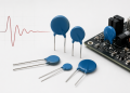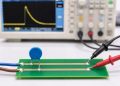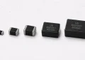
An SMD MOV—a surface-mount device (SMD) implementation of a metal-oxide varistor (MOV)—is a voltage-dependent protection component designed for direct assembly onto a printed circuit board (PCB). It remains highly resistive during normal operation and conducts strongly when a transient voltage exceeds its nonlinear operating region.
The name “SMD MOV” sounds precise, but it is actually an umbrella term. It may describe a multilayer ceramic chip varistor, a molded surface-mount device containing an MOV disc, or another metal-oxide construction adapted for automated assembly. These products can differ greatly in operating voltage, capacitance, surge capability and intended circuit position.
Key point: select an SMD MOV by its construction and electrical ratings, not by the words “SMD” or “MOV” alone.
SMD MOV Terminology
- SMD — Surface-Mount Device: a component designed for direct mounting onto the surface of a printed circuit board rather than insertion through drilled holes.
- MOV — Metal-Oxide Varistor: a voltage-dependent resistor, commonly based on zinc oxide, used to limit transient overvoltage.
- SMD MOV — Surface-Mount Metal-Oxide Varistor: an umbrella term for MOV constructions adapted for surface mounting.
- SMD varistor / surface-mount varistor: describes the mounting form but does not always identify the internal material or construction.
- Chip varistor: often refers to a compact multilayer product, although some catalogs use the term more broadly.
- MLV — Multilayer Varistor: one important SMD MOV construction, but not every SMD MOV is an MLV.
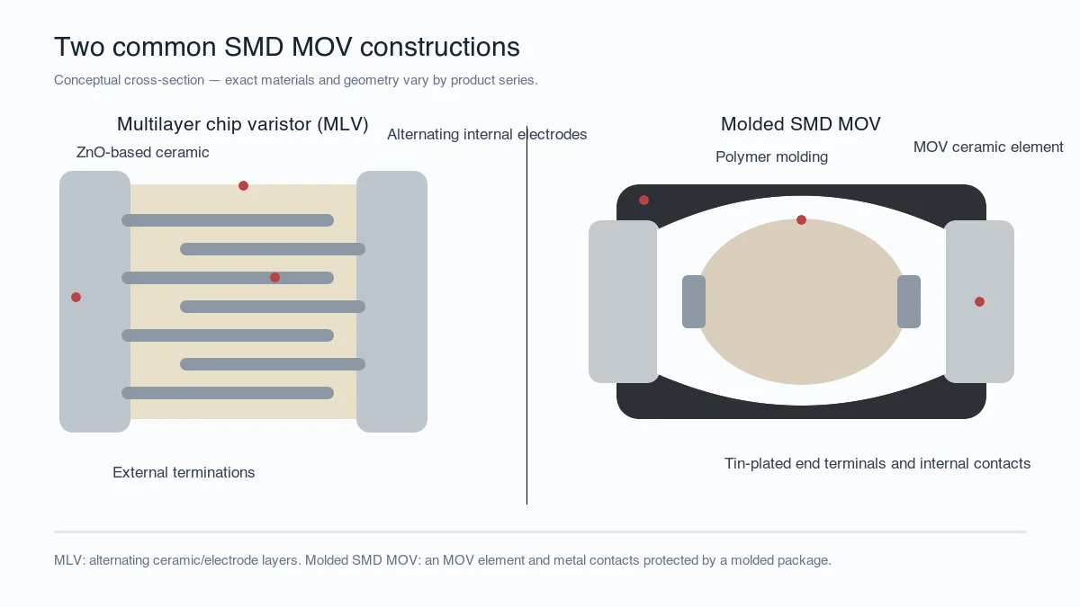
- Molded SMD MOV: may contain a monolithic MOV element or disc with metal terminals inside a molded package.
- SMD disc varistor: uses a disc-like active element with external terminals designed for surface mounting.
Supplier listings sometimes use these names interchangeably. When the name is ambiguous, check the cross-section, package drawing, capacitance, surge rating and recommended application in the datasheet.
How Does an SMD MOV Work?
The active metal-oxide ceramic contains many conductive zinc-oxide grains separated by electrically active grain boundaries. At normal voltage, the grain boundaries restrict current. When the electric field becomes sufficiently high, many boundaries conduct at once and current rises nonlinearly.
The SMD MOV is normally connected in parallel with the circuit or line being protected. During a transient it diverts current away from the sensitive load and limits the voltage to a residual clamping level. After a pulse within its rating, it returns to a high-resistance state.
This behavior is bidirectional. A standard MOV has no positive or negative terminal and can suppress transients of either polarity. However, the protected circuit still sees the clamping voltage plus any voltage created by PCB trace inductance.
The Main SMD MOV Constructions
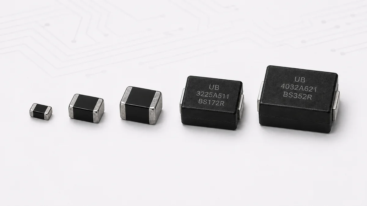
1. Multilayer ceramic varistor
A multilayer varistor uses alternating semiconducting ceramic layers and internal electrodes. It is leadless, compact and commonly supplied in chip sizes such as 0402, 0603, 0805, 1206, 1210 or larger, depending on the series.
MLVs are widely used for board-level electrostatic discharge (ESD), electrical fast transient (EFT) and switching-transient protection. Their capacitance can range from low values for selected signal-line products to much higher values for power and control-line products. Their surge capability also varies substantially by package and construction.
2. Molded monolithic or disc-based SMD MOV
Some surface-mount MOVs place a larger metal-oxide element inside a molded package with metal terminals. Compared with a small MLV, this construction may support higher continuous voltages, surge currents and energies and may be intended for primary-side or power-input protection.
The larger body and thermal mass require attention to reflow profile, land pattern, board spacing and heat transfer. The device may look like another molded passive component, so identification from appearance alone is unreliable.
3. Specialized and hybrid constructions
Manufacturers also offer low-capacitance arrays, feedthrough-style products, automotive-qualified MLVs and hybrid protectors. A hybrid may combine MOV behavior with another protection technology. These products should not be treated as ordinary two-terminal SMD MOVs without reviewing their circuit and pin configuration.
SMD MOV, MLV and Chip Varistor: Are They the Same?
They overlap but are not exact synonyms:
| Term | What it tells you | What it does not guarantee |
|---|---|---|
| SMD MOV | Surface-mount format and metal-oxide varistor behavior | Multilayer structure, package size or energy class |
| MLV | Multilayer ceramic varistor construction | Low capacitance, automotive rating or high surge capability |
| Chip varistor | Compact chip-style package | Exact material or internal geometry |
| Molded SMD MOV | Molded surface-mount body | Whether the active element is multilayer or disc based |
Where Is an SMD MOV Used?
Typical applications include:
- Low-voltage power rails near microcontrollers, sensors and interface ICs
- Connectors, buttons and other points exposed to ESD
- Automotive modules, subject to the required qualification and pulse ratings
- Industrial control and communication equipment
- Light-emitting diode (LED) lighting controls and auxiliary supplies
- Consumer electronics and smart-home products
- Switching power supplies and alternating-current (AC) inputs when a suitable high-voltage SMD MOV is specified
Placement matters. A board-level MLV near a connector and a high-energy molded SMD MOV at a power input may both be called SMD MOVs, but they solve different problems.
Important Electrical Parameters
Maximum continuous alternating-current (AC) and direct-current (DC) voltage
The maximum continuous voltage is the highest voltage that may be applied continuously under specified conditions. AC and DC ratings are different and should not be converted using a simple square-root relationship. Allow for supply tolerance, charging voltage, abnormal but expected operating states and temperature.
Varistor voltage
Varistor voltage is measured at a defined DC current, commonly 1 milliampere (mA) for many MOV families but sometimes a different current for small chip products. It is a production reference point, not the normal operating voltage and not the clamping voltage.
Clamping voltage
Clamping voltage is the maximum residual voltage at a stated pulse current and waveform. The test current used for a small MLV may be very different from that used for a larger molded MOV. Compare clamping values only when the conditions are comparable.
Peak surge current and energy
Peak current is normally tied to a waveform such as 8/20 μs. Energy may be specified with a longer pulse such as 10/1000 μs or another defined condition. A single-pulse maximum does not describe repetitive endurance. Use the pulse-count or derating curves when available.
Capacitance
Capacitance is especially important for SMD MOVs because some are placed on signal lines. High capacitance can distort fast interfaces, while controlled capacitance may help filter slower control or power lines. Check the measurement frequency and bias conditions.
Leakage current
Leakage influences standby power, battery life and high-impedance measurements. It rises with applied voltage and temperature and can increase after overstress. Review the specified limit at the intended operating point.
Package, termination and temperature
Confirm case size, land pattern, termination material, reflow compatibility, operating temperature and board-flex requirements. Automotive-grade or sulfur-resistant claims apply only when explicitly stated for the selected part.
How to Select an SMD MOV
- Define the normal AC or DC voltage, including maximum tolerance.
- Identify the transient: ESD, EFT, switching spike, lightning surge or automotive pulse.
- Determine the waveform, source impedance, peak current and pulse count.
- Set the maximum residual voltage that the downstream circuit can tolerate.
- Choose the construction: small MLV, molded high-energy SMD MOV or specialized device.
- Compare clamping curve, surge endurance, capacitance and leakage.
- Check temperature derating, package, reflow and qualification.
- Validate the complete PCB in the required system-level test.
PCB Placement and Layout
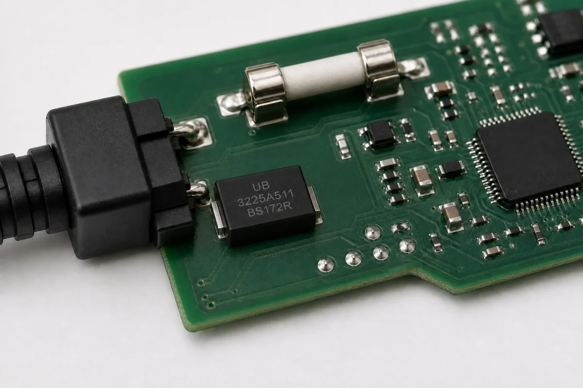
Place the SMD MOV close to the transient entry point. Route the transient path through the protector before it branches toward the sensitive circuit. Keep the path to the return node short and wide enough for the expected pulse current.
Long traces add inductive voltage. Even a fast component cannot clamp effectively if the surge current must travel through a long loop. On high-energy inputs, observe creepage, clearance, fuse coordination and thermal spacing.
Reliability and Failure Modes
Possible failure mechanisms include ceramic cracking, termination damage, solder-joint failure, leakage increase, varistor-voltage shift, thermal runaway, short circuit and open circuit. The most common design causes are excessive continuous voltage, a surge above the rated waveform, too many repetitive pulses, poor thermal coordination and PCB flex.
An MOV subjected to sustained abnormal overvoltage may continue conducting and overheat. Power-line designs may therefore require an upstream fuse, thermal disconnect or a thermally protected MOV solution. Never assume that the MOV alone provides safe disconnection.
Common Selection Mistakes
- Selecting by varistor voltage while ignoring maximum continuous voltage
- Comparing clamping voltages measured at different currents
- Assuming every SMD MOV is a low-voltage MLV
- Using a high-capacitance device on a fast signal line
- Using a board-level ESD part for a high-energy power surge
- Ignoring repetitive pulse endurance and temperature derating
- Copying a package-compatible part without comparing construction and curves
Frequently Asked Questions
Does an SMD MOV have polarity?
No. A standard metal-oxide varistor is bidirectional.
Is a larger SMD package always stronger?
Not necessarily. A larger active volume often supports more pulse energy, but construction, voltage grade and internal geometry also matter. Use the datasheet ratings.
Can an SMD MOV replace a transient-voltage-suppression (TVS) diode?
Sometimes, but not automatically. Compare operating voltage, clamping curve, capacitance, leakage, polarity behavior and pulse waveform. Each technology has different strengths.
Can an SMD MOV be used directly across an AC line?
Only when the specific device is rated for that AC voltage, surge environment, safety requirements and assembly process. Many small MLVs are intended only for low-voltage board-level protection.
What is the difference between 0805 and 1206 SMD MOVs?
The numbers describe approximate imperial package dimensions, not electrical ratings. Voltage, capacitance and surge capability still depend on the product series.
Conclusion
SMD MOV is a broad name covering several surface-mount metal-oxide varistor constructions. Small multilayer chips are widely used for local ESD and transient protection, while molded or disc-based SMD MOVs may handle higher-energy power surges. Correct selection begins by identifying the actual construction and transient waveform, then comparing continuous voltage, clamping behavior, pulse endurance, capacitance, leakage and assembly requirements.
For the basic voltage terminology used throughout this article, see What Is a Varistor? MOV Basics and Key Parameters. Final suitability should always be confirmed against the manufacturer’s current datasheet and the real system test.