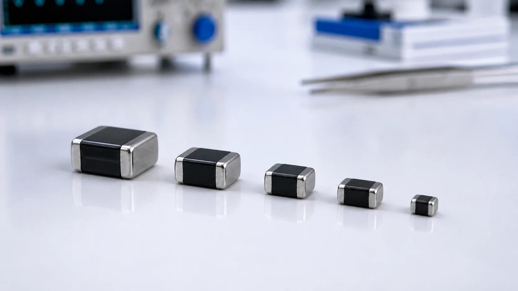
Electronic circuits can be damaged by electrostatic discharge (ESD), switching transients and other short overvoltage events. A multilayer varistor (MLV; Chinese: 多层片式压敏电阻) is a compact surface-mount component designed to divert these transient currents and limit the voltage reaching sensitive circuitry.
In short: an MLV is a bidirectional, voltage-dependent ceramic protection device. It combines multiple active ceramic layers and internal electrodes in a small leadless package, making it especially useful for board-level protection where space is limited.
MLV Terminology and Common Names
The same product family may appear under several English and Chinese names. They overlap, but they are not always completely interchangeable:
- MLV — Multilayer Varistor: the standard English abbreviation and full name. The most precise Chinese translation is 多层片式压敏电阻.
- Multilayer Chip Varistor: frequently used by component manufacturers to emphasize the chip package. Chinese names include 多层片式压敏电阻 and 多层芯片压敏电阻.
- Multilayer Ceramic Varistor: emphasizes the ceramic construction. It may be translated as 多层陶瓷压敏电阻.
- Chip Varistor / SMD Varistor: broader commercial terms, translated as 片式压敏电阻 or 贴片压敏电阻. These names describe the mounting form and do not always prove that the internal construction is multilayer.
- SMD MOV: means a surface-mount metal-oxide varistor. An MLV belongs to this broad family, but “SMD MOV” can also be used loosely for other surface-mount constructions.
- ESD suppressor: a functional name used for low-capacitance or IC-level protection products. Not every ESD suppressor is an MLV, and not every MLV is intended only for ESD.
For technical communication and search consistency, this article uses MLV (multilayer varistor / 多层片式压敏电阻) as the primary term. When reviewing a supplier listing, confirm the datasheet construction rather than relying on a translated product name.
What Is an MLV?
MLV stands for multilayer varistor. Like other metal-oxide varistors, it has a nonlinear voltage-current characteristic. Under normal operating voltage, the device presents high resistance and draws very little current. When the voltage rises above its operating region, its resistance drops rapidly, allowing transient current to bypass the protected circuit.
Unlike a traditional leaded disc MOV, an MLV is manufactured as a multilayer ceramic chip. Alternating layers of semiconducting ceramic and internal metal electrodes create many active junctions inside the component. This construction provides useful transient suppression in a compact surface-mount format.
An MLV is inherently bidirectional, so it can respond to positive and negative transients without the orientation requirement of a unidirectional diode. However, its exact voltage, energy, capacitance and surge capability depend strongly on the product series and package size.
Most MLVs use a zinc-oxide-based semiconducting ceramic system with carefully controlled additives. Their protective action is created mainly at the boundaries between ceramic grains. The exact formulation, electrode system and firing process are manufacturer-specific and directly affect voltage gradient, leakage current, nonlinear coefficient, capacitance and reliability.
How Does an MLV Work?
The behavior of an MLV can be understood in three operating regions:
- Normal operation: the applied voltage is below the device’s continuous operating limit. The MLV remains in a high-resistance state and has minimal influence on the circuit.
- Transient event: a voltage spike pushes the device into its nonlinear conduction region. Current is redirected through the MLV and the voltage across the protected node is limited.
- After the event: when the transient disappears, the MLV returns to its high-resistance state, provided that the pulse remained within its rated capability.
The MLV does not remove all transient voltage. It clamps the event to a lower level. The actual clamping voltage depends on the surge current, waveform, device impedance and parasitic inductance in the printed circuit board (PCB) layout. For this reason, a clamping-voltage value is meaningful only together with its specified test current and waveform.
Why Zinc-Oxide Ceramic Becomes Voltage Dependent
A sintered metal-oxide varistor contains many conductive zinc-oxide grains separated by electrically active grain boundaries. At low voltage, these boundaries restrict current and the device behaves like a high resistance. As the electric field increases, the barriers at many grain boundaries break down together and current rises sharply.
This produces the nonlinear relationship commonly approximated as I = K × Vα, where the nonlinear coefficient α indicates how sharply current increases with voltage. The equation is useful for understanding behavior, but practical selection should use the manufacturer’s measured voltage-current curve and specified clamping values.
In an MLV, many thin ceramic layers allow the required voltage characteristic to be achieved in a small chip. Layer thickness, grain size, electrode overlap and the number of active layers all influence the final electrical behavior.
Inside the Multilayer Structure
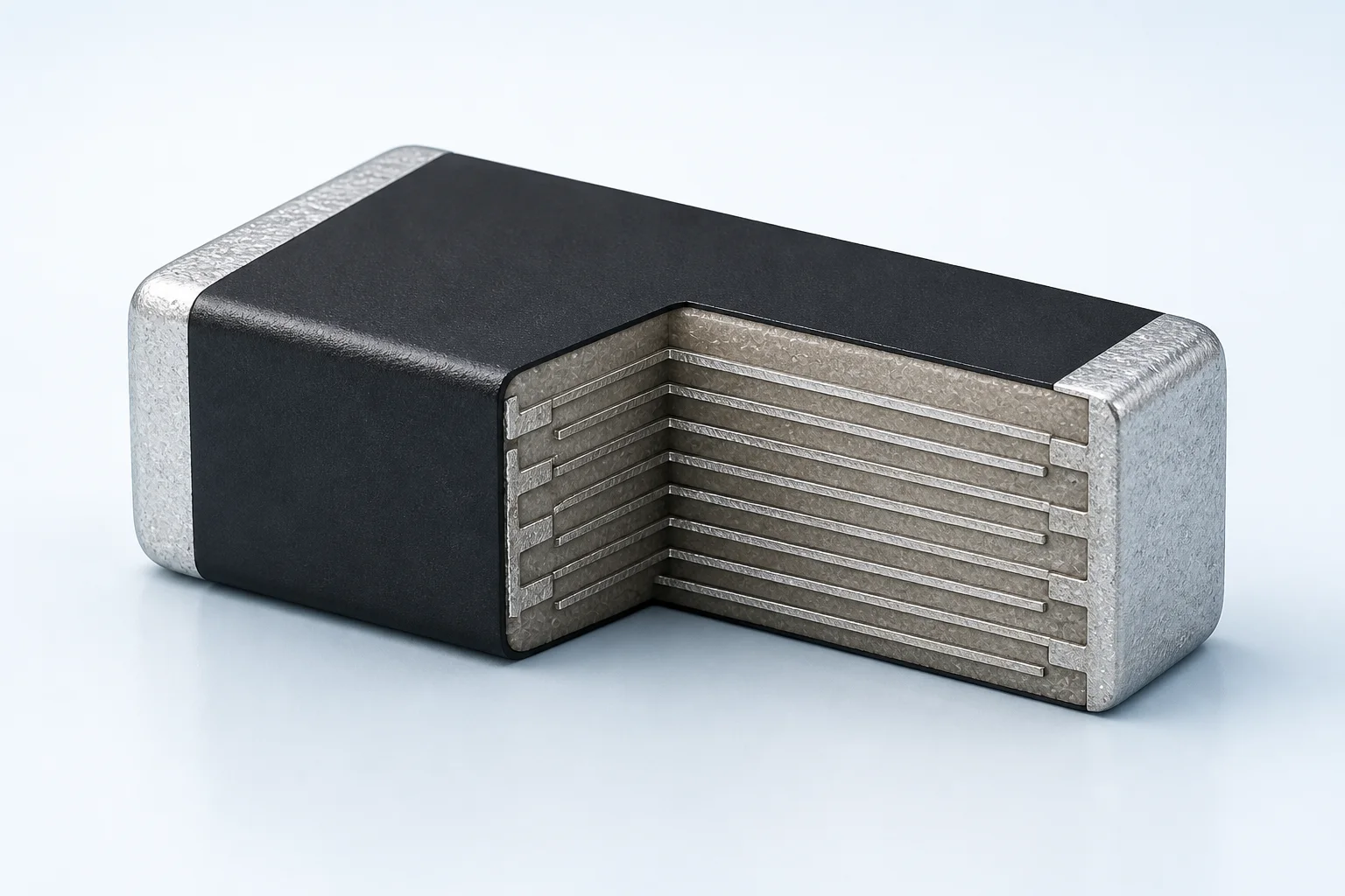
A typical MLV contains four functional parts:
- Semiconducting metal-oxide ceramic layers
- Interleaved internal electrodes
- External terminations for surface mounting
- A protective outer coating or termination finish, depending on the series
The overlap between the internal electrodes creates many active varistor regions in parallel. Increasing the effective electrode area and changing the ceramic formulation, layer thickness and number of layers allows the manufacturer to tune voltage, capacitance and pulse-handling characteristics.
This internal geometry is also why two MLVs in the same package size may have very different electrical ratings. Package dimensions alone cannot be used to select an equivalent part.
How an MLV Is Manufactured
Manufacturing details vary, but a typical process includes ceramic-powder preparation, slurry formation, tape casting, internal-electrode printing, layer stacking, lamination, cutting, binder removal, co-firing, termination and electrical sorting. The ceramic body and internal electrodes must shrink and densify compatibly during firing.
This is more than a packaging process. Small changes in ceramic chemistry, layer thickness, electrode geometry or firing conditions can change the varistor voltage, leakage current and pulse endurance. For that reason, an apparent package-compatible replacement still requires electrical and reliability verification.
Electrode materials may differ between manufacturers and product generations. Silver, silver-palladium and other systems can be used, but no electrode composition or firing temperature should be inferred without the specific manufacturer’s technical data.
Understanding the Voltage-Current Curve
The characteristic curve can be divided into three practical regions:
- Pre-breakdown or leakage region: current is very small and is strongly affected by voltage and temperature.
- Nonlinear operating region: current increases rapidly while voltage rises more slowly. Varistor voltage and clamping behavior are characterized here.
- High-current region: bulk resistance, electrodes, terminations and parasitic inductance become increasingly important. Excess energy can cause irreversible damage.
Three voltage terms are therefore different: the maximum continuous operating voltage is the normal-use limit; the varistor voltage is a reference measurement at a defined current; and the clamping voltage is the residual voltage under a stated pulse current. Treating these three values as the same is a common selection error.
MLV, Disc MOV and Transient-Voltage-Suppression (TVS) Diode: What Is the Difference?
| Device | Typical construction | Common role | Important consideration |
|---|---|---|---|
| MLV | Multilayer ceramic SMD chip | Board-level ESD, EFT and transient suppression | Capacitance and pulse capability vary widely by series |
| Leaded disc MOV | Metal-oxide ceramic disc with leads | Power-input and higher-energy surge protection | Usually larger; ratings must match the mains or DC bus |
| TVS diode | Semiconductor junction device | Fast transient clamping with defined unidirectional or bidirectional options | Polarity, breakdown behavior and surge waveform must be checked |
These are not universal substitutes for one another. A compact MLV can be an excellent choice near a connector, sensor or control IC, while a disc MOV may be better suited to a high-energy input surge. A TVS diode may be preferred when the circuit requires a tightly controlled semiconductor clamping characteristic. Some designs use more than one protection stage.
For a broader introduction to varistor terminology, see What Is a Varistor? MOV Basics and Key Parameters.
Main Advantages of MLVs
- Compact SMD package: suitable for automated PCB assembly and dense layouts.
- Bidirectional protection: responds to transients of either polarity.
- Fast nonlinear response: useful for short ESD, EFT and switching events.
- Wide design range: available in different voltage, capacitance, package and surge classes.
- Local protection: can be placed close to connectors, IC supply rails, sensors and control lines.
Limitations to Consider
An MLV should not be selected only because it is small. Important limitations include:
- Capacitance: standard MLVs may load high-speed signal lines. Low-capacitance series are available, but the datasheet value must be checked against the interface requirement.
- Energy capability: many MLVs are intended for board-level transients rather than repeated high-energy mains surges.
- Clamping level: the protected IC must tolerate the residual voltage at the relevant pulse current.
- Cumulative stress: repeated pulses near or above the rating can change leakage or varistor characteristics over time.
- Mechanical stress: ceramic chips can crack if the PCB bends or the assembly process is poorly controlled.
Degradation and Failure Modes
An MLV is reusable after pulses that remain within its rating, but it is not immune to aging. Repeated or excessive stress can gradually increase leakage current, shift the varistor voltage or eventually create a short or open circuit. Possible failure mechanisms include:
- Thermal damage from excessive continuous voltage or sustained abnormal current
- Localized ceramic breakdown after a pulse above the current or energy rating
- Electrode or termination damage caused by extreme current density
- Cracking from PCB flex, depanelization, impact or unsuitable land patterns
- Solder-joint or termination problems caused by poor reflow control
- Parameter drift after a large number of pulses close to the endurance limit
A protection design should consider both the single-pulse maximum and the expected lifetime pulse profile. If a fault can apply continuous power after the MLV begins conducting, additional current limiting, fusing or system-level protection may be necessary.
Typical MLV Applications
MLVs are commonly considered in the following areas, subject to series-specific ratings:
- Power and ground lines near microcontrollers and mixed-signal ICs
- Buttons, keypads, connectors and exposed user interfaces
- Sensor inputs and industrial control lines
- Automotive electronic modules and low-voltage vehicle networks
- Consumer electronics, appliances and smart-home products
- LED lighting control and auxiliary power circuits
- Telecommunications and data interfaces when capacitance is acceptable
Automotive qualification, load-dump capability and high-temperature operation should never be assumed from the term “MLV” alone. They apply only to products specifically designed and qualified for those conditions.
ESD, EFT and Surge Are Not the Same Test
Protection terms are often mixed together in marketing descriptions, but the stress waveforms are different:
- ESD (electrostatic discharge): a very fast, short event commonly evaluated at system level using IEC 61000-4-2 or a customer-specific method.
- EFT/burst (electrical fast transient): repetitive fast pulses, often associated with switching of inductive loads and commonly evaluated using IEC 61000-4-4.
- Surge: a slower, higher-energy transient such as the combination-wave tests associated with IEC 61000-4-5.
- Automotive transients: pulses defined by vehicle electrical conditions and standards such as ISO 7637-2 or manufacturer-specific requirements.
A device that performs well in one test is not automatically suitable for another. Compare the actual waveform, source impedance, pulse count, polarity and temperature with the component rating and the system requirement.
Key Parameters for MLV Selection
1. Maximum continuous operating voltage
The normal AC or DC operating voltage must stay below the manufacturer’s specified continuous-voltage rating, including tolerance, charging conditions and expected supply variation.
2. Varistor voltage
Varistor voltage is measured at a defined test current. Many datasheets use a DC current such as 1 mA, but the actual test current can vary by product family. It is a reference point for the nonlinear characteristic, not the voltage that the protected circuit will necessarily see during a surge.
3. Clamping voltage
Clamping voltage is specified at a stated pulse current and waveform. Compare that value with the absolute maximum voltage of the downstream circuit, while allowing margin for layout inductance and component tolerance.
4. Surge-current and energy rating
Check the pulse shape, peak current, pulse duration and allowed number of events. A rating based on an 8/20 μs waveform cannot be directly treated as the same as a longer-energy waveform or continuous overload.
5. Capacitance
Capacitance may be useful for filtering on power or slower control lines, but excessive capacitance can distort high-speed signals. Review the capacitance at the stated frequency and bias condition when the protected node carries data.
6. Leakage current
Leakage matters in battery-powered equipment, high-impedance sensing and other low-power circuits. Check it at the actual operating voltage and temperature.
7. Package and temperature range
Confirm the package size, land pattern, termination finish, soldering process, operating temperature and any required qualification such as AEC-Q200. Larger packages may offer greater pulse capability, but the datasheet remains the final reference.
8. Tolerance and voltage-current curve
Do not compare only nominal varistor voltage. Review the stated tolerance and the upper and lower voltage-current curves. The worst-case clamping level must still protect the load, while the lowest possible conduction level must not create unacceptable leakage during normal operation.
9. Pulse endurance and derating
Check both the maximum single pulse and repetitive-pulse curves when available. Voltage, current and energy derating may be required at elevated temperature. If the datasheet does not define the expected pulse condition, ask the manufacturer to confirm suitability.
10. Qualification and reliability evidence
AEC-Q200, IEC test references, RoHS/REACH declarations and reliability reports describe different aspects of the product. AEC-Q200 is a component qualification framework, not a guarantee that every automotive electrical pulse is covered. Match the evidence to the actual application requirement.
A Practical Selection Process
- Define the normal operating voltage and its worst-case tolerance.
- Identify the transient source: ESD, EFT, switching spike, surge or automotive pulse.
- Define the relevant waveform, current and number of expected events.
- Set the maximum voltage that the protected circuit can tolerate.
- Compare continuous voltage, clamping voltage, pulse rating, leakage and capacitance.
- Check package, temperature, qualification and assembly requirements.
- Verify the design with the actual PCB and the required system-level test.
PCB Layout and Assembly Notes
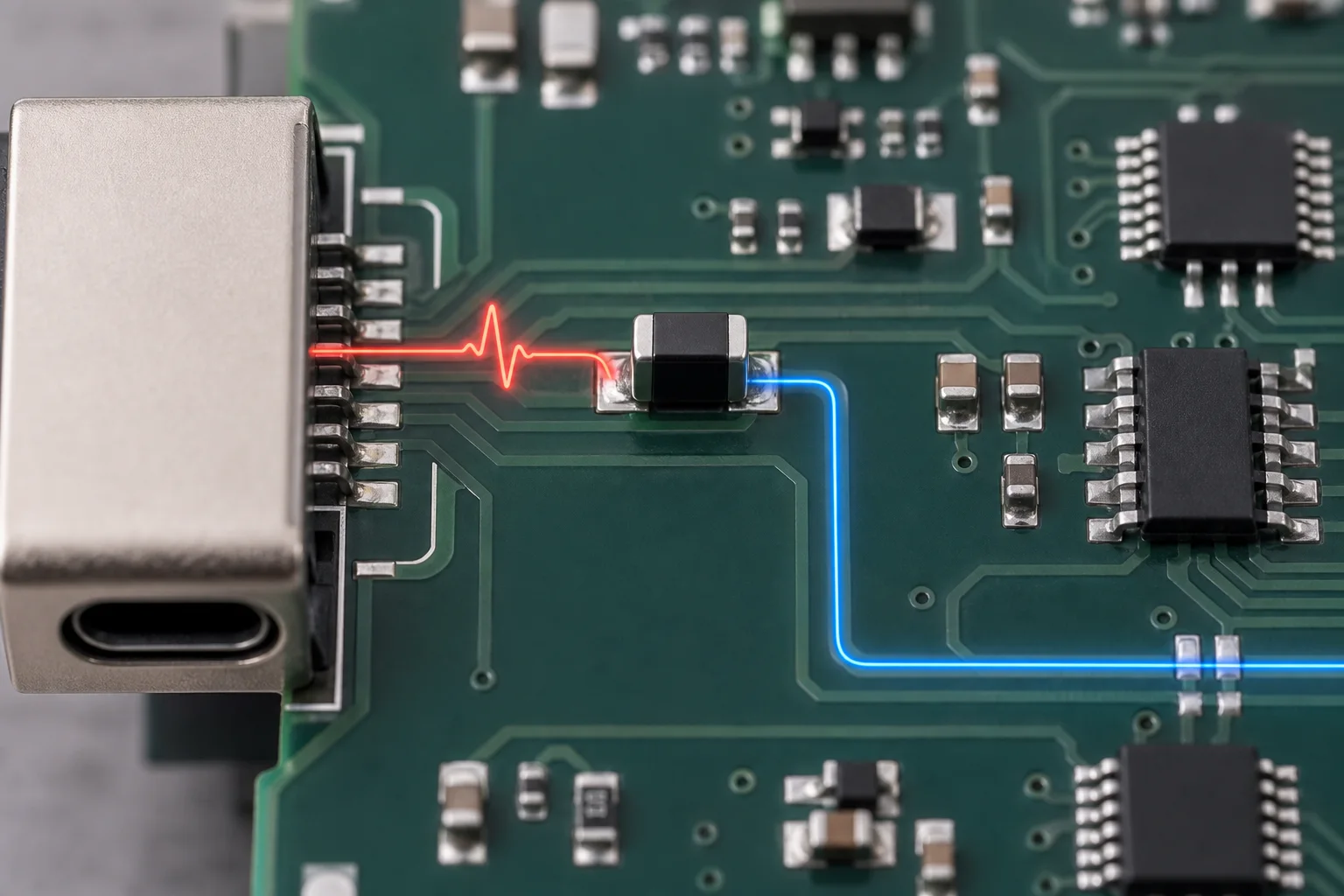
Protection performance depends on placement as well as component rating. Keep the connection between the transient entry point, MLV and return path short and low in inductance. Avoid long branches that allow the transient to reach the protected circuit before it reaches the suppressor.
For signal protection, place the component close to the connector or exposure point. For supply protection, use a return path appropriate to the system grounding strategy. Follow the manufacturer’s land-pattern, reflow and board-flex recommendations because excessive mechanical or thermal stress can damage multilayer ceramic components.
Frequently Asked Questions
Is an MLV the same as an SMD MOV?
An MLV is a type of surface-mount metal-oxide varistor made with a multilayer ceramic structure. “SMD MOV” is a broader description and may be used for different surface-mount constructions. Check the manufacturer’s construction and datasheet instead of relying only on the name.
Are “chip varistor,” “multilayer chip varistor” and “MLV” identical?
“Multilayer chip varistor” and MLV normally describe the same construction. “Chip varistor” is less precise because it can be used as a general package description. In Chinese purchasing documents, 贴片压敏电阻, 片式压敏电阻, 多层压敏电阻 and 多层片式压敏电阻 may all appear; the datasheet construction and electrical ratings should be used to resolve the meaning.
Can an MLV protect a mains input?
Only if a specific product is rated for the operating voltage, surge waveform, energy and safety requirements of that application. Many MLVs are designed primarily for low-voltage board-level protection and should not be substituted for a mains-rated MOV.
Can an MLV be used on a high-speed data line?
Sometimes. The deciding factor is usually capacitance together with the interface bandwidth and signal-integrity margin. Use a suitably low-capacitance device and validate the complete interface.
Does an MLV have polarity?
No. Its voltage-dependent behavior is bidirectional, so a standard MLV does not have positive and negative terminals.
Can two parts with the same size and varistor voltage be substituted?
Not automatically. Also compare continuous voltage, varistor-voltage tolerance, clamping curve, test current, surge waveform, capacitance, leakage, pulse endurance, temperature range, termination and qualification. A valid cross-reference requires condition-by-condition comparison.
Conclusion
An MLV combines nonlinear metal-oxide protection with a compact multilayer surface-mount structure. It is particularly useful for local ESD, EFT and transient suppression around connectors, control circuits and sensitive electronics. Successful selection requires more than matching a nominal voltage: continuous voltage, clamping conditions, pulse waveform, capacitance, leakage, package and qualification must all be considered together.
For related fundamentals, see What Is a Varistor? and What Is an SMD MOV?. The final choice should always be confirmed against the manufacturer’s datasheet and validated under the actual system test conditions.