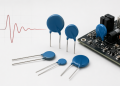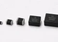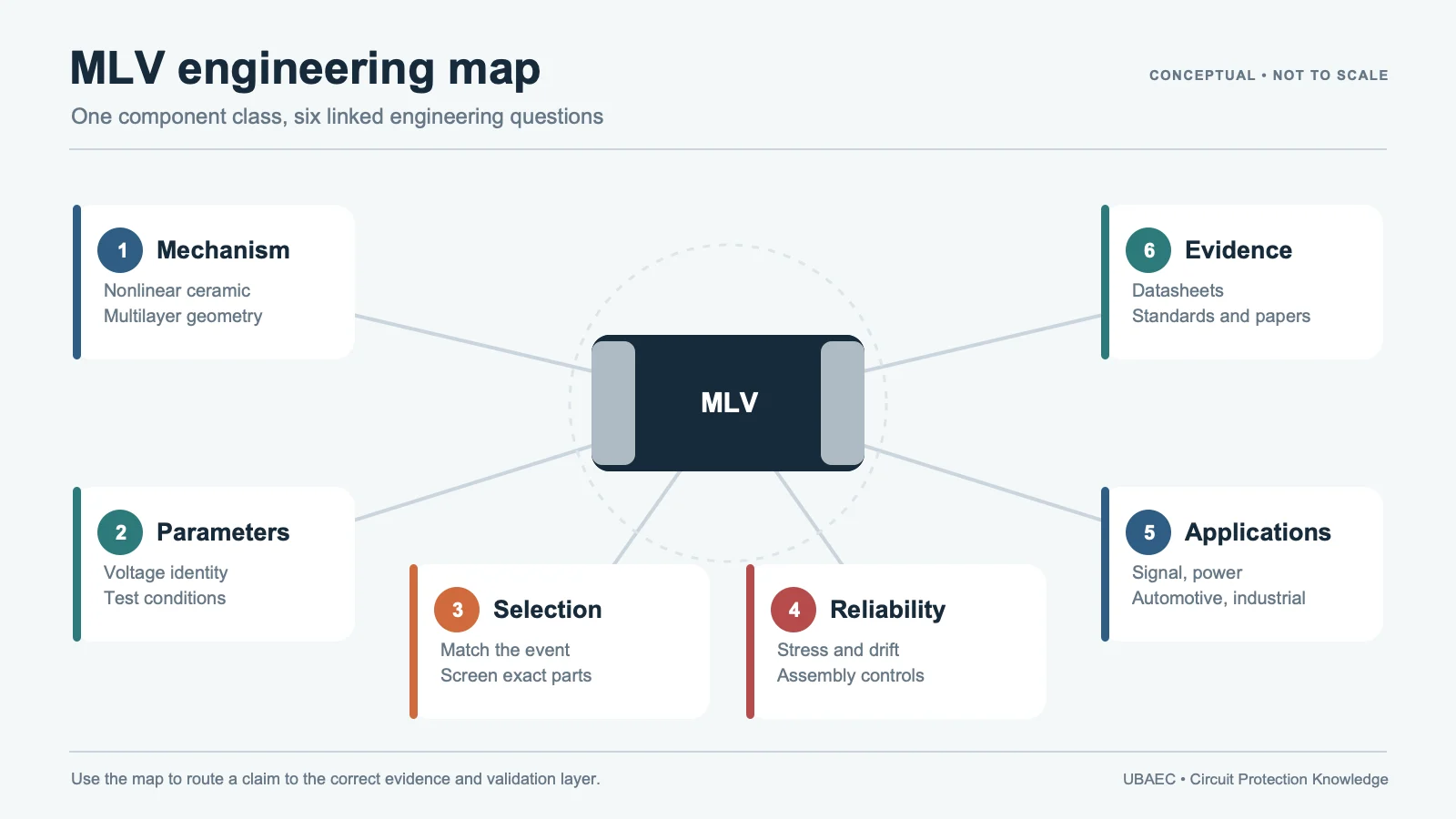
Quick answer: a multilayer varistor (MLV) is a construction class, while a metal-oxide varistor (MOV) describes a broader material and device family. Surface-mount device (SMD) and chip describe form or mounting, array describes topology, and electrostatic discharge (ESD) suppressor describes a protection role. These terms can overlap, but they are not interchangeable.
The safest engineering rule is to verify the construction first, identify the package and topology second, and compare electrical ratings only after those boundaries are clear.
This article focuses on terminology and classification boundaries. For the complete topic path, start with the MLV Knowledge Map.
Why MLV Terminology Becomes Ambiguous
Component catalogs often mix several classification levels in one product title. A name may describe what a device does, what it is made from, how it is built, how it mounts, how many protection elements it contains or which commercial family it belongs to. A distributor category or translated title may simplify the wording even further.
This creates avoidable errors. A surface-mount varistor may be assumed to be a ceramic MLV, an array may be treated as a single two-terminal part, or a current rating from a molded MOV may be transferred into a chip-varistor comparison. None of those conclusions is justified by the name alone.
A Six-Layer Method for Classifying Varistors
Before comparing parts, separate the product description into six layers:
- Function: nonlinear voltage-dependent resistance, transient suppression, ESD protection or filtering.
- Material or technology: metal-oxide ceramic, semiconductor avalanche, polymer/composite, resin/thick-film or gas discharge.
- Construction: multilayer ceramic, disc, molded or plastic-encapsulated surface-mount structure, diode structure or another verified design.
- Package or mounting: chip, SMD, radial leaded, leadless multi-terminal or another package form.
- Topology: discrete two-terminal device, independent multi-element array, shared-terminal array or protection-plus-filter network.
- Commercial name: a manufacturer-owned series, trademark or portfolio label.
A product title may answer only one or two of these questions. Use the current manufacturer datasheet, product page and construction document to resolve the remaining layers.
MLV, MLCV, MOV, Chip Varistor and CTVS Explained
| Term | What the term identifies | Relationship to an MLV | Safe use |
|---|---|---|---|
| Varistor or voltage-dependent resistor (VDR) | A nonlinear voltage-dependent device function | An MLV is one varistor construction | Add the verified material and construction before discussing ratings |
| Metal-oxide varistor (MOV) | A broad metal-oxide ceramic device family | Many commercial MLVs are MOVs, but MOV does not define one package or construction | Qualify the term as multilayer, disc, molded SMD or another confirmed form |
| Multilayer varistor (MLV) | A multilayer nonlinear ceramic construction with internal electrodes and external terminations | The core construction class covered by this article | Use exact series and order-code evidence for every rating or qualification claim |
| Multilayer chip varistor (MLCV) | A multilayer varistor name that emphasizes chip form | Often used as a form-qualified synonym for MLV | Retain the manufacturer’s wording and confirm the construction in its official document |
| Chip varistor | A common product or package label | Frequently refers to an MLV, but the words alone are not sufficient construction evidence | Confirm the multilayer ceramic structure before aggregation or cross-reference |
| Ceramic transient voltage suppressor (CTVS) | A manufacturer or category term for ceramic varistor protection in the cited context | May overlap with an MLV or chip-varistor portfolio | Retain the source context; do not expand CTVS into transient voltage suppressor diode |
TDK describes ceramic multilayer varistors as CTVS devices and explains their alternating ceramic and electrode layers. Panasonic describes a chip varistor as a chip-shaped laminated ceramic varistor. These official descriptions support the overlap among MLV, chip-varistor and ceramic-suppressor wording, but the exact manufacturer document must still control the classification of a particular series.
Why an SMD Varistor Is Not Automatically an MLV
Surface-mount device describes mounting and package form, not internal construction. A surface-mount varistor may be:
- a bare multilayer ceramic MLV;
- a molded or plastic-encapsulated MOV;
- a disc-like or monolithic varistor element adapted to surface mounting;
- a multi-element array or integrated filter structure; or
- a product whose construction is not established by the public title.
The distinction is visible in first-party documentation. The KEMET VP datasheet identifies a plastic-encapsulated surface-mount varistor and describes it as a surface-mount equivalent to selected leaded disc varistors. Eaton’s official MOVS page likewise identifies a surface-mount MOV family; that page now marks the family discontinued, so it is useful as a construction and lifecycle example rather than a current design recommendation.
Neither example should be placed in a bare ceramic-MLV parameter matrix solely because it is surface mounted. The detailed comparison belongs in MLV vs SMD MOV and Disc MOV.
MLV, Molded SMD MOV and Disc MOV Boundaries
| Construction class | Typical physical form | Evidence needed | Boundary rule |
|---|---|---|---|
| Multilayer ceramic varistor | Leadless ceramic chip with internal electrodes and wraparound end terminations | Current MLV series or order-code datasheet | Use only the conditions stated for that exact series or part |
| Molded or plastic-encapsulated SMD MOV | Rectangular molded body with metal terminals on two opposing ends | Construction drawing, series datasheet and lifecycle record | Do not transfer its ratings to a bare ceramic MLV |
| Disc or radial MOV | Coated or encapsulated ceramic disc with radial leads | Exact disc-series datasheet and applicable safety information | Do not transfer surge, energy, mains or safety ratings to an MLV |
Some manufacturers offer higher-voltage or higher-energy MLV families. That does not make alternating-current mains protection a generic MLV capability. Exact working voltage, transient waveform, repetition, thermal behavior, failure mode, safety evidence and system coordination still determine whether a specific product is suitable.
ESD Suppressor Is a Role, Not a Construction
An ESD suppressor may be an MLV, a transient voltage suppressor (TVS) diode, a semiconductor diode array, a polymer/composite suppressor or another technology. The functional label does not establish the device material, capacitance, dynamic clamping behavior or suitability for a particular interface.
| Term | Technology or role | Relationship to an MLV |
|---|---|---|
| TVS diode | Semiconductor avalanche protection device | An alternative or complementary technology, not an MLV |
| ESD diode array | Multiple semiconductor protection junctions in one package | Not an MLV array even when the channel count looks similar |
| Polymer, composite or resin suppressor | A non-ceramic suppression technology | Requires separate construction and pulse-behavior evidence |
| Gas discharge tube (GDT) | A gas-discharge protection device | A different device that may be used in a coordinated protection stage |
Detailed technology comparisons should use exact parts under matched operating voltage, source impedance, waveform, clamp current, repetition, temperature and printed circuit board (PCB) conditions. The MLV vs TVS Diode guide demonstrates this method for two widely used protection technologies.
Arrays and Filtered MLVs Need a Topology Definition
An MLV array integrates two or more varistor elements in one body. The elements may be independent or may share terminals. Per-line ratings, package-level ratings and test configurations are not automatically interchangeable.
The Littelfuse MLN SurgeArray datasheet, for example, describes four independent suppressors in one leadless multilayer chip and reports ratings for an individual section. That topology cannot be reduced to the word “array” without retaining the per-section scope.
A filtered or feedthrough MLV combines transient suppression with a frequency-dependent filtering structure. It is not equivalent to a plain two-terminal MLV. Pinout, equivalent circuit, capacitance balance, insertion loss and bandwidth require exact model evidence.
Trade Names and Portfolio Names
Names such as TransGuard, ChipGuard and ZNR identify manufacturer-owned families or portfolios; they are not generic construction classes. A portfolio may include more than one technology, and a family name may continue across revisions or lifecycle changes.
The KYOCERA AVX TransGuard datasheet, for example, explicitly identifies the family as multilayer ceramic transient voltage suppressors. The manufacturer attribution and datasheet construction make that classification defensible. A distributor category, photograph or abbreviated title would not be an equivalent substitute.
How to Classify a Part Before Comparing Ratings
- Record the exact manufacturer, series and complete order code.
- Locate the current official product page, datasheet and construction document.
- Separate function, material, construction, package and topology into different fields.
- Record whether the source is current, historical, regional, translated or superseded.
- Keep an unresolved construction outside any MLV parameter aggregation.
- Only then compare continuous alternating-current (AC) and direct-current (DC) voltage, varistor voltage and test current, clamping voltage and pulse current, surge waveform, repetitions, energy waveform, capacitance conditions, leakage, temperature and qualification.
A package code or nominal varistor voltage is not enough for a cross-reference. The MLV Datasheet Parameters and Test Conditions guide explains how to preserve the measurement conditions during the next stage.
Frequently Asked Questions
Is an MLV the same as an MOV?
Not exactly. MOV is a broader metal-oxide varistor family, while MLV identifies a multilayer construction. In technical comparisons, add the construction and exact series instead of using MOV as a universal package label.
Are MLV and MLCV interchangeable terms?
They are often used for the same multilayer chip-varistor class, but manufacturers do not use the acronyms uniformly. Preserve the manufacturer’s term and confirm the construction in its official document.
Is every chip varistor or SMD varistor an MLV?
No. Chip and SMD describe form or mounting. A product can instead be molded, plastic encapsulated, disc-derived, integrated with another function or insufficiently documented. Construction evidence must decide the classification.
Does CTVS mean TVS diode?
No. In the cited TDK context, CTVS refers to a ceramic transient voltage suppressor based on multilayer-varistor technology. A TVS diode is a semiconductor avalanche device.
Can ratings be transferred between MLV, molded SMD MOV and disc MOV?
No. Working voltage, clamping voltage, surge current, energy, pulse endurance, safety status and temperature limits remain tied to the exact construction, series, order code and test conditions.
Summary
MLV identifies a multilayer construction. MOV identifies a broader metal-oxide varistor family. Chip and SMD describe form or mounting. ESD suppressor describes a role. Array describes topology. CTVS and trade names require manufacturer context. Keeping these levels separate prevents incorrect parameter transfer, weak cross-references and unsafe application assumptions.
Return to the MLV Knowledge Map for the structured path through fundamentals, parameters, selection, applications, reliability and technical resources.
Continue Reading
- How Multilayer Varistors Work
- MLV vs SMD MOV and Disc MOV
- How to Cross-Reference MLVs Safely
- MLV Knowledge Map
Official Technical References
- TDK Electronics — Multilayer Varistors: MLV construction and CTVS terminology.
- Panasonic Industry — Basics of Surge/ESD and Protection Components: chip-varistor, surge-absorber and ESD-suppressor boundaries.
- KYOCERA AVX — TransGuard Multilayer Ceramic Transient Voltage Suppressors: manufacturer family and construction terminology.
- KEMET — VP Plastic Encapsulated Surface Mount Varistors: molded/plastic-encapsulated SMD MOV boundary.
- Eaton — MOVS Surface-Mount Metal-Oxide Varistors: historical construction and lifecycle boundary; the official page currently marks the family discontinued.
- Littelfuse — MLN SurgeArray Suppressor Datasheet: multi-element topology and per-section rating scope.
These references support terminology and construction boundaries. They do not create part equivalence, prove current availability or transfer a rating between product families. Verify the current document revision and lifecycle before design release.