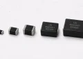
A multilayer varistor (MLV) is not created by placing an ordinary varistor inside a chip package. Its electrical behavior emerges from the ceramic material, grain-boundary microstructure, internal-electrode geometry, co-firing process, terminations and final controls working as one system.
This page gives a general technical overview. It does not describe a supplier’s commercial formula or production settings. For the electrical mechanism, read How Multilayer Varistors Work.
The Material System: What Can Be Said Publicly
Many MLV families use a zinc-oxide-based semiconducting ceramic with controlled secondary constituents. During processing and sintering, the system develops conductive grains and electrically active grain boundaries that create nonlinear voltage-current behavior.
The words ZnO based do not identify a complete formulation. Additive identity and concentration, powder characteristics, binder system, electrode material, atmosphere and thermal profile can differ by manufacturer, product family and generation. Public content should therefore separate a generic material-class explanation from a product-specific claim.
Why Microstructure Matters
The electrical path crosses many grains and grain boundaries. Grain size distribution, boundary chemistry, porosity, phase distribution and defects can influence the voltage gradient, leakage, nonlinearity, capacitance, current concentration and degradation behavior.
Research papers help explain these relationships. Published work on varistor ceramics describes the grain-boundary basis of nonlinear behavior, while laboratory work on zinc-oxide chip-varistor specimens exposed to electrostatic discharge reports stress-related barrier changes. These are mechanism findings for the studied materials and conditions, not proof that every commercial MLV uses the same formulation or has the same robustness.
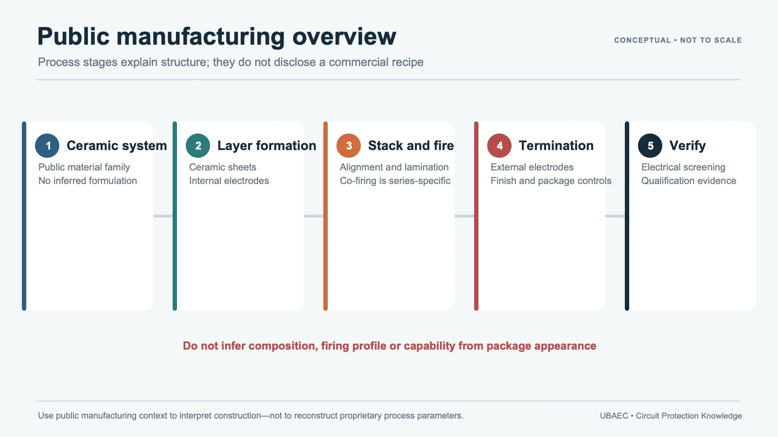
General MLV Manufacturing Flow
1. Ceramic powder and slurry preparation
Raw ceramic powders and process additives are prepared and dispersed into a slurry suitable for forming thin sheets. Particle distribution, dispersion and contamination control matter because nonuniformity can carry into the fired microstructure.
2. Tape casting or sheet formation
The slurry is formed into thin green ceramic sheets. Thickness uniformity affects the later electrical geometry, but no universal layer thickness should be inferred across suppliers or series.
3. Internal-electrode printing
Electrode patterns are printed on selected sheets. Registration, print quality and material compatibility affect overlap, current distribution and co-firing behavior. The actual electrode system is proprietary unless the manufacturer publishes it for the exact product.
4. Stacking, lamination and cutting
Printed and unprinted sheets are aligned, stacked and laminated into a consolidated green body, then separated into chip-sized parts. Alignment and lamination defects can change active geometry or create mechanical weak points.
5. Binder removal and co-firing
Organic constituents are removed and the ceramic/electrode structure is fired. Densification, grain development, phase formation and electrode compatibility occur through a controlled thermal and atmospheric process. A patent or academic example may disclose one claimed route; it does not prove another manufacturer uses that route.
6. External termination and surface protection
External terminations connect alternate internal electrodes to opposite ends of the part. Plating or other finish layers support soldering and environmental performance. Some designs also use surface-protection or passivation approaches. The exact stack and materials remain series-specific.
7. Electrical testing, sorting and inspection
Finished parts are measured and sorted using manufacturer-defined controls. Relevant checks may include dimensional and visual inspection, reference varistor voltage, leakage, capacitance and other product-specific tests. The public datasheet or quality document—not a generic process diagram—defines the released specification and sampling basis.
How Process Choices Connect to Electrical Behavior
| General process/material factor | Possible electrical or reliability connection | Evidence caution |
|---|---|---|
| Grain and boundary development | Nonlinearity, voltage gradient, leakage and degradation behavior | Material-system and specimen dependent |
| Active ceramic thickness and electrode overlap | Voltage behavior, capacitance and current distribution | Exact geometry is product specific |
| Porosity, inclusions or registration defects | Local field/current concentration and mechanical weakness | Requires process/inspection evidence |
| Termination and passivation | Solderability, surface leakage, environmental and mechanical behavior | Does not by itself prove surge or ESD rating |
| Firing atmosphere and thermal profile | Densification, phase development and electrode compatibility | Proprietary process window; no public recipe inference |
How to Read Papers and Patents Correctly
Academic papers are useful for physical mechanisms, test observations and historical context. Patents describe claimed inventions and possible routes. Neither evidence class automatically proves that a current commercial product uses the disclosed design or achieves the described benefit.
For example, patent literature discusses field-optimized microstructures and surface-passivation approaches. Those documents can show that such ideas were claimed and explain their intended technical purpose. Patent status is jurisdiction-specific, and the disclosure does not establish commercialization, mass-production yield, current qualification or an exact product rating.
A public product statement requires corroboration from current manufacturer documentation tied to the exact family or order code. Treat research papers, patents, historical documents and current product specifications as separate evidence classes.
Manufacturing Quality Is Not One Datasheet Number
Manufacturing consistency may appear indirectly through tolerance, leakage limits, voltage-current curves, endurance tests, mechanical tests, environmental qualification and process-control documentation. A single nominal varistor voltage or package size does not describe the complete distribution or failure risk.
For selection, use the MLV datasheet parameters and test-conditions guide. For degradation and evidence layers, use MLV reliability, standards and failure modes. Assembly can also damage an otherwise conforming ceramic chip, so review the MLV layout, mounting and soldering guide.
Questions for a Supplier or Technical Review
- Which official document confirms the exact series and current revision?
- Which construction and termination information is publicly supported?
- What conditions define Vvar, leakage, capacitance, clamping and pulse endurance?
- Which tests apply to the exact order code and package?
- What derating, soldering, board-flex and environmental controls apply?
- Does a claimed process or patent have current product corroboration?
Summary
MLV behavior is the result of a coupled material-and-structure system: nonlinear ceramic microstructure, multilayer electrodes, co-firing, terminations, surface protection and final control. General process stages can be explained publicly, but formulas, electrode systems, layer geometries and process windows remain product- and manufacturer-specific unless current first-party evidence says otherwise.
Continue Reading
- How Multilayer Varistors Work
- MLV Datasheet Parameters and Test Conditions
- MLV Reliability, Standards and Failure Modes
- MLV PCB Layout, Mounting and Soldering
Official Technical References
The following first-party, standards-organization or publisher records support the technical boundaries used in this article. Always verify the current revision and the exact product scope before design release.
- Varistor Ceramics
- Degradation of potential barriers in ZnO-based chip varistors due to electrostatic discharge
- Multilayer Varistors technology and product overview
- Basics of chip varistors and comparison with other protection devices
- WO2020007864A1 – Multilayer varistor having a field-optimized microstructure
- DE112019003625T5 – Varistor passivation layer and process for its manufacture