A multilayer varistor (MLV) protects a circuit through two ideas working together: a nonlinear ceramic material whose conductivity changes strongly with voltage, and a multilayer electrode geometry that places many active regions inside a compact chip.
This article explains the mechanism at an engineering-concept level. For naming and construction boundaries, use the MLV terminology guide; for the complete topic path, use the MLV Knowledge Map.
The Short Working Principle
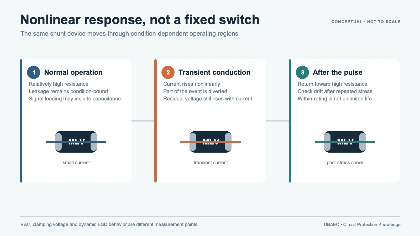
At normal circuit voltage, an MLV is in a relatively high-resistance region. When a transient raises the electric field, current through the device increases nonlinearly. Connected as a shunt across a protected node, the MLV diverts part of the transient current and limits the node voltage. After an in-rating event ends, it returns toward its pre-event high-resistance behavior.
“Limits” is more accurate than “holds at a fixed voltage.” The residual voltage depends on the exact device, pulse current and waveform, tolerance, temperature and PCB path impedance.
Why the Ceramic Is Voltage Dependent
Many commercial MLVs use zinc-oxide-based varistor ceramics. The sintered body contains conductive grains separated by electrically active grain boundaries. At low field, these boundaries restrict current. As the field increases, the boundary barriers become much more conductive and the current rises sharply.
A common physical model describes electrically active grain boundaries as barrier regions with nonlinear behavior. A current path crosses many such boundaries, and their collective response produces the steep voltage-current characteristic associated with a varistor. A peer-reviewed overview of varistor ceramics discusses this grain-boundary model.
This model is useful for understanding the class, but it is not a product recipe. Additives, grain size distribution, electrode materials, firing conditions and passivation are manufacturer- and series-specific. Academic results for one specimen or material system cannot establish the composition or performance of a commercial part.
What the Multilayer Geometry Adds
Inside a typical chip, alternating internal electrodes connect to opposite external terminations. Where the electrodes overlap, the nonlinear ceramic between them forms active varistor regions. Multiple regions operate together within the component.
The geometry lets manufacturers tune an MLV family through material and structural choices such as effective electrode area, active ceramic thickness and the arrangement of active regions. Those choices influence voltage behavior, capacitance, current distribution and robustness. They must not be reverse-engineered from package size or a marketing photograph.
The related materials, microstructure and manufacturing overview explains the general process stages without turning patents or research papers into a commercial process claim.
Three Operating Regions on a Conceptual Voltage-Current (V-I) Curve
1. Pre-conduction or leakage region
Below the intended continuous operating limit, current is relatively small. It is not zero and can vary with applied voltage, temperature, material state and the exact measurement method. Leakage matters in low-power and high-impedance circuits.
2. Nonlinear transition and clamping region
As voltage rises, current increases much faster than voltage. A reference varistor voltage is measured at a stated current, while clamping voltage is measured at a stated pulse current and waveform. These are different points and cannot be substituted for each other.
3. High-current region
At higher current, bulk resistance, electrodes, terminations, heating and circuit inductance become increasingly important. The voltage continues to rise, and excessive electrical or thermal stress can cause irreversible change or failure.
Use the MLV datasheet parameters and test-conditions guide for the formal meanings of working voltage, varistor voltage, clamping voltage, current, energy, capacitance and leakage.
How Current Is Diverted in a Circuit
An MLV is normally connected between the exposed node and an appropriate return path. During a transient, current divides between the intended protection path and every other available path. The MLV can only control the portion of the event that reaches it through the printed circuit board (PCB) network.
Connection inductance produces additional voltage during fast current change. Long traces, large loops or a poor return path can therefore raise the voltage at the protected device even when the MLV itself has a suitable datasheet curve. Placement close to the entry point and a short diversion path are part of the protection function, not merely assembly preferences.
The MLV layout, mounting and soldering guide owns the detailed PCB and mechanical controls.
Why an MLV Also Looks Capacitive
Alternating electrodes separated by ceramic create capacitance. That capacitance is part of the device’s small-signal behavior and can affect signal rise time, insertion loss or filtering. It may be acceptable or useful on a power or slower control line and unacceptable on a high-speed interface.
Capacitance is not one universal MLV value. It varies by series and order code and must be read with the stated measurement frequency and, where relevant, bias and temperature conditions.
What Happens After a Pulse?
If the event remains within the product’s capability, the MLV should return toward its high-resistance state. That does not mean unlimited pulses produce no change. Published laboratory research on ZnO-based chip varistors under ESD stress reports changes involving grain-boundary barriers and electrical behavior in the tested specimens.
The result depends on material system, specimen geometry, pulse network, amplitude, count, bias, measurement method and time after stress. Such research does not define a universal International Electrotechnical Commission (IEC) 61000-4-2 rating or commercial lifetime. Product endurance data and final-system tests remain controlling.
See MLV reliability, standards and failure modes for single-pulse, repetitive-stress, mechanical and qualification evidence layers.
Five Common Misunderstandings
- “The MLV switches at one exact voltage.” Its response is a nonlinear curve with tolerance and test-condition dependence.
- “Clamping voltage is the same as varistor voltage.” They are measured at different current and waveform conditions.
- “Fast response removes PCB effects.” Interconnect inductance and return-path geometry still affect residual voltage.
- “The multilayer structure defines one capacitance or pulse rating.” Exact families can differ widely.
- “An academic mechanism proves product capability.” Product ratings require current manufacturer evidence for the exact series or order code.
Engineering Questions to Carry into Selection
- What is the normal maximum voltage at the node?
- What transient source, waveform, source impedance and repetition apply?
- How much residual voltage can the protected circuit tolerate?
- What capacitance and leakage can the circuit accept?
- Where will transient current return, and how short is that path?
- What degradation, temperature, qualification and final-system tests are required?
Summary
An MLV works because electrically active ceramic grain boundaries become strongly conductive as the electric field rises, while a multilayer electrode structure creates compact active regions and useful board-level form factors. The device diverts current and limits voltage along a condition-dependent curve; capacitance, layout and cumulative stress remain part of the real behavior.
Continue Reading
- MLV Materials, Microstructure and Manufacturing
- MLV Datasheet Parameters and Test Conditions
- MLV Reliability, Standards and Failure Modes
- MLV PCB Layout, Mounting and Soldering
Official Technical References
The following first-party, standards-organization or publisher records support the technical boundaries used in this article. Always verify the current revision and the exact product scope before design release.
- Multilayer Varistors technology and product overview
- Basics of chip varistors and comparison with other protection devices
- Varistor Ceramics
- Degradation of potential barriers in ZnO-based chip varistors due to electrostatic discharge
- Electrical Degradation Caused by Electro-Static Discharge Pulse in ZnO-Based Multilayer Varistor
- Safety precautions for chip-type multilayer varistors