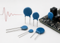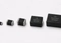
“ESD suppressor,” “chip protector” and “surface-mount protection device” describe a role or package, not one construction. The component may be a ceramic multilayer varistor, a resin/thick-film structure, a polymer/composite suppressor or a semiconductor device.
Construction evidence comes before performance comparison. Similar size and marketing language do not make these devices interchangeable, and a low-capacitance or fast-response label does not prove suitability for a particular interface.
Use the MLV terminology and product-boundary guide when a product title does not clearly identify the underlying technology.
Three Different Evidence Classes
| Class | General construction | Typical evidence needed | Boundary |
|---|---|---|---|
| Ceramic MLV | Nonlinear ceramic layers with embedded internal electrodes and external terminations | Official MLV technology page plus exact series/order-code datasheet | Core UBAEC MLV class |
| Resin/thick-film suppressor | Substrate, printed or thick-film electrodes and a resin/composite transient path, exact design dependent | Construction drawing or material/process statement for the exact family | Separate from ceramic MLV aggregation |
| Polymer/composite ESD suppressor | Non-ceramic polymer or composite transient path | Exact family datasheet covering capacitance, dynamic behavior, repetition and temperature | Alternative technology, not an MLV |
Resin/thick-film and polymer/composite devices should not automatically be merged with each other. The manufacturer may use different materials and structures, so public copy should retain the exact family description rather than inventing one universal category.
Why Construction Documents Outrank Category Labels
NIC’s NXED web category has used MLV-related wording. Its construction document, however, describes an alumina substrate, thick-film electrodes, glass and absorbent resin. Because the construction evidence is more specific than the category label, UBAEC treats NXED as a separate resin/thick-film suppressor and excludes its ratings from the ceramic MLV matrix.
This is not a criticism of the product. It is a classification rule that prevents values from one technology being presented as if they describe another. The same rule applies to distributor taxonomies, translated titles and package photographs.
“ESD Suppressor” Does Not Define Technology
A current Semiware category page visibly separates MLV, semiconductor-diode and polymer suppressor categories. Bourns’ ChipGuard portfolio also illustrates that one commercial umbrella can include construction-confirmed MLV families and non-varistor thin-film polymer devices.
Therefore, always write the underlying technology: ceramic MLV, polymer ESD suppressor, resin/thick-film suppressor or TVS/ESD diode. The MLV vs TVS diode guide owns the semiconductor comparison, while MLV vs SMD/disc MOV owns the MOV construction boundary.
Compare Exact Parts, Not Category Slogans
| Attribute | What to record | Common mistake |
|---|---|---|
| Continuous voltage | Maximum operating voltage, polarity/configuration, tolerance and temperature | Using a trigger or test voltage as the normal rail |
| Clamp behavior | Injected current/network, waveform, fixture, polarity and dynamic overshoot | Comparing unrelated ESD and surge clamp values |
| Capacitance | Maximum/typical value, frequency, amplitude, DC bias and temperature | Treating “low capacitance” as an interface guarantee |
| Leakage | Applied voltage, temperature and test limit | Comparing values measured at different bias points |
| Pulse duty | Pulse shape, source impedance, repetition, interval and acceptance criteria | Converting one ESD event into repetitive or surge capability |
| Lifecycle | Ageing/drift evidence, storage/operating limits and failure state | Calling one technology universally non-ageing or failsafe |
The MLV parameter guide provides the detailed field definitions. Use the exact polymer or resin-device datasheet to create corresponding fields; do not assume it uses the MLV parameter vocabulary.
Capacitance and High-Speed Lines
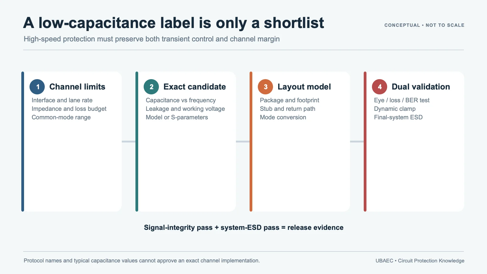
Polymer/composite suppressors are often marketed for very-low-capacitance applications, while MLV capacitance can range widely by size and family. That tendency is not a substitute for exact maximum values and channel-level testing.
For a high-speed line, compare capacitance with frequency and bias, insertion loss or S-parameters where available, dynamic clamp behavior, leakage, package parasitics and layout. Then run eye-diagram or equivalent signal-integrity testing and system ESD validation. Interface-specific decisions belong in the high-speed port protection guide.
Pulse Repetition, Ageing and Failure State
Ceramic, polymer/composite and resin/thick-film structures can respond differently to repeated stress, temperature and humidity. Public comparisons should not turn one supplier’s selected test into a universal lifetime rule.
Ask what was stressed, how many times, at what interval and temperature, and what counted as failure. Monitor leakage, reference/trigger voltage, clamp behavior or other technology-appropriate parameters before and after stress. Coordinate the protection system for the possible degraded state.
Matched-Condition Selection Checklist
- Record the exact manufacturer, family, order code, revision and lifecycle state.
- Verify ceramic MLV, resin/thick-film, polymer/composite or semiconductor construction.
- Define normal rail, signal bandwidth and protected-circuit absolute limits.
- Define the ESD/transient source, network, waveform, source impedance and repetition.
- Compare clamp behavior at matched conditions rather than a single headline number.
- Compare maximum capacitance, frequency/bias, leakage and signal-integrity evidence.
- Check temperature, humidity, ageing, package, assembly and failure behavior.
- Validate the exact device on the final PCB and document any unresolved evidence gap.
The MLV selection workflow provides a general engineering sequence. Use the MLV Technical Resources & Datasheet Library and the official manufacturer or publisher links below, then verify the exact family, revision, lifecycle and test conditions.
Summary
MLV, resin/thick-film and polymer ESD suppressor are construction-level distinctions. ESD suppressor and SMD are role/package umbrellas. Classify first, then compare exact parts under matched voltage, clamp, capacitance, leakage, pulse, temperature and lifetime conditions. Do not turn NIC NXED or another non-ceramic family into MLV range data.
Return to the MLV Knowledge Map for the complete route through terminology, parameters, selection, reliability and applications.
Continue Reading
- MLV vs TVS Diode: How to Compare Protection Devices
- MLV vs SMD MOV and Disc MOV
- High-Speed Port ESD Protection: MLV, TVS and Low-Capacitance Trade-Offs
- How to Select an MLV: A Practical Engineering Workflow
Official Technical References
The following first-party, standards-organization or publisher records support the technical boundaries used in this article. Always verify the current revision and the exact product scope before design release.
- Multilayer Varistors technology and product overview
- Basics of chip varistors and comparison with other protection devices
- NXED MLV Transient Voltage Suppressor
- NXED Surface Mount ESD Suppressor datasheet and construction record
- Bourns ChipGuard ESD Suppressors product hub
- ESD Protection Devices
- ESD Suppressor product hub