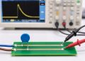
An MLV array is not simply “several MLVs in a smaller package.” Multi-element devices can use independent sections, shared terminals, differential pairing or protection-plus-filter structures. Pinout and internal topology determine the current path, coupling and rating scope.
The practical rule: identify technology and topology separately, then determine whether every value is per element, per line or for the complete package.
The MLV terminology guide explains why an MLV array is also different from a semiconductor ESD-diode array.
Four Topology Classes
| Topology | General structure | Key benefit or role | Evidence risk |
|---|---|---|---|
| Discrete two-terminal MLV | One nonlinear element between two terminations | Simple line-to-ground or line-to-line placement | Two separate parts are not automatically matched |
| Multi-element MLV array | Two or more varistor elements integrated in one body | Multi-line integration and potentially controlled element relationships | Common-terminal and independent-element arrays are not interchangeable |
| Matched/differential multi-element device | Two or more sections intended for a defined bus or paired-line topology | Compact paired protection with product-specific balance claims | A selected 2-in-1 device is not evidence for two discrete MLVs |
| Feedthrough or ESD/EMI filter device | Transient-suppression elements combined with a feedthrough, LC or other frequency-dependent path | Protection plus conducted/radiated EMI control | Equivalent circuit, feedthrough current and bandwidth must be exact-model specific |
Technology and Array Count Are Separate
A ceramic MLV array integrates nonlinear varistor elements in a multilayer body. An ESD-diode array integrates semiconductor junctions and may include steering diodes or rail clamps. A polymer-array product would use another technology. Similar channel count or IC-like packaging does not create equivalence.
Record both fields: technology and topology. Then confirm the pinout and whether the current returns to ground, another line, a shared node or an internal filtering path.
Independent, Shared-Terminal and Differential Structures
KYOCERA AVX MultiGuard documentation demonstrates that array configuration and common-terminal topology must remain visible. Littelfuse MLN documentation describes multiple independent varistor sections in one package and separately publishes surge-clamp and ESD-clamp information. These are family examples, not universal array definitions.
A shared-terminal array may reduce component count but also makes the common-node inductance and return path important. An independent-element package provides a different routing model. A differential or matched 2-in-1 part may have product-specific capacitance-balance or common-mode-range claims that cannot be assumed for two unrelated discrete parts.
Per-Line, Per-Element and Package Ratings
Before using a table, label every value with its scope:
- continuous voltage per protected line or element;
- varistor voltage and test current per element;
- clamping voltage at a stated current and waveform;
- peak current or energy per element, simultaneous-channel or package total;
- capacitance per line, element matching/tolerance and inter-channel coupling;
- ESD result for the component, mounted device or complete system;
- maximum common/feedthrough current where a signal or power path passes through the part.
If the datasheet does not define simultaneous-channel behavior, do not multiply a per-line value by the number of elements. The MLV parameter guide owns the voltage, waveform and clamp definitions.
Feedthrough and Protection-Plus-Filter Devices
A feedthrough MLV does more than place a shunt varistor beside a signal. Its multi-terminal geometry creates an intended through path and a frequency-dependent suppression/filtering function. KYOCERA AVX TransFeed documentation, for example, requires the four-pad layout, maximum feedthrough current and product-specific capacitance and pulse conditions to remain together.
Check the equivalent circuit, pin numbering, DC resistance, rated through current, capacitance, insertion loss or S-parameters, cutoff behavior and grounding geometry. Do not replace the device with a two-terminal MLV based on voltage and package size alone.
Lifecycle and Application Scope Cannot Be Transferred
Panasonic’s legacy EZJZS high-speed 2-array material and its current EZJPR-M automotive 2-in-1 product have different lifecycle, topology, purpose and conditions. One cannot serve as evidence for the other. Archive sources may explain history, but current exact product data controls selection.
The same rule applies across interfaces. CAN/CAN FD evidence does not automatically prove RS-485, USB or another bus. Application pages must retain the exact interface, transceiver, common-mode range, capacitance/balance and system test plan.
Pinout and PCB Layout
The protection path should be short and intentional from the connector or transient entry point to the return node. In an array, one shared return trace can add common impedance between channels. In a feedthrough part, swapping input/output or bypassing the intended pad geometry can change the filter behavior.
Use the exact land pattern and orientation. Verify which pads are signal, ground, common or no-connect, and keep the return path separated from sensitive internal ground where required by the system architecture. See the MLV PCB layout guide.
Selection and Validation Checklist
- Confirm MLV, diode, polymer or other underlying technology.
- Draw the exact internal topology and external pinout.
- Label ratings as per line, per element, simultaneous-channel or package level.
- Match continuous voltage, Vvar test current, clamp current/waveform and pulse duty.
- Record capacitance, frequency/bias, tolerance, balance and inter-channel coupling.
- For feedthrough devices, record DC/through current and insertion-loss or S-parameter data.
- Confirm lifecycle, qualification scope, temperature and exact land pattern.
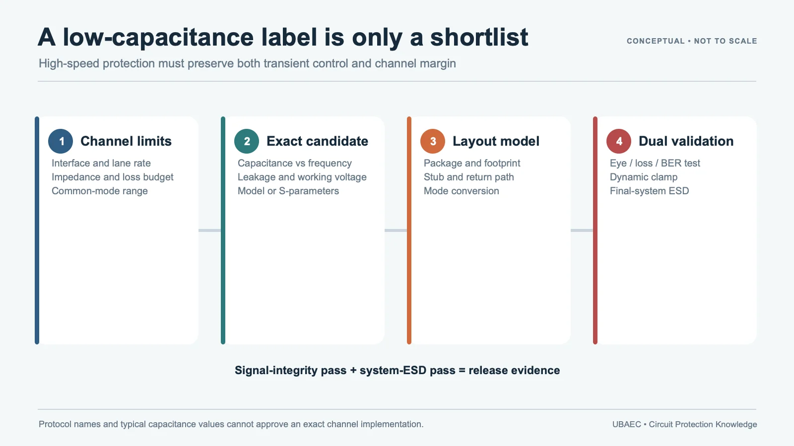
- Measure per-line clamp, crosstalk and signal integrity on the final PCB.
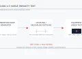
- Run the applicable component and system ESD/transient tests with the real interface.
Use the MLV selection workflow for the broader process. Interface-level decisions belong in the CAN and CAN FD protection guide and the high-speed port protection guide; neither application page turns one array topology into a universal bus solution.
Summary
Discrete, array, differential/matched and feedthrough/filter MLVs are different topologies. Channel count does not define technology, and one array’s ratings do not automatically apply per line or to the full package. Keep pinout, current path, capacitance balance, waveform, feedthrough current, lifecycle and final-system validation together.
Review the official documents listed below and verify the exact product revision and lifecycle. Use the MLV Technical Resources & Datasheet Library for the maintained source index, or return to the MLV Knowledge Map.
Continue Reading
- MLV Terminology and Product Boundaries
- MLV Datasheet Parameters and Test Conditions
- CAN and CAN FD Protection with Multi-Element MLVs
- How to Select an MLV: A Practical Engineering Workflow
Official Technical References
The following first-party, standards-organization or publisher records support the technical boundaries used in this article. Always verify the current revision and the exact product scope before design release.
- MultiGuard Series multilayer varistor array datasheet
- MLN Series Varistor Datasheet
- TransFeed multilayer feedthrough varistor datasheet
- Automotive multilayer varistors EZJZ-M, EZJP-M and EZJPR-M 2-in-1
- IEC 61000-4-2:2025 – Electromagnetic compatibility (EMC) – Part 4-2: Testing and measurement techniques – Electrostatic discharge immunity test
- ISO 10605:2023 – Road vehicles – Test methods for electrical disturbances from electrostatic discharge