“High-speed port” is not one electrical interface. HDMI, DisplayPort, USB 3.x, USB4 and other differential links have different channel, pin, mode and compliance requirements. A protection device that works on one lane or data rate is not automatically suitable for another.
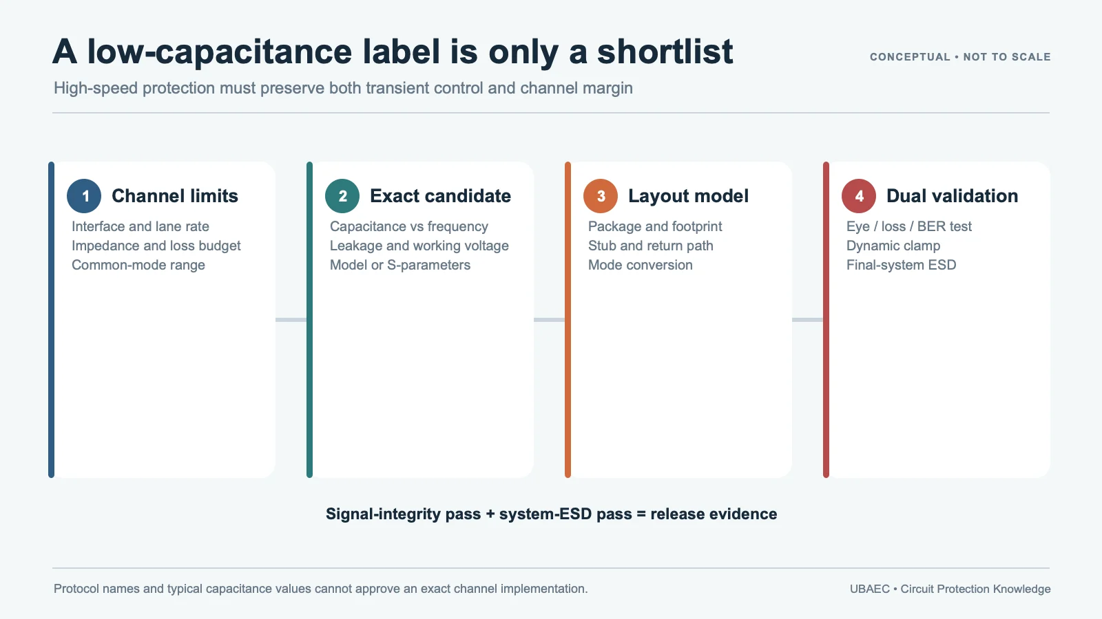
Low capacitance is only the first gate. The selected MLV, TVS/ESD diode array, polymer/composite suppressor or other device must also meet the voltage window, dynamic-clamp need, leakage, package and signal-integrity limits in the exact PCB channel.
Map the Port Before Choosing a Technology
List every exposed conductor and assign its function: high-speed differential lane, lower-speed control/sideband line, power, configuration/identification, shield or ground. Record data rate, signaling voltage, common-mode range, differential impedance, lane polarity/orientation switching, AC coupling and protected-IC limits.
Do not apply one “USB-C protector” to every Type-C pin from a single table. The same connector can carry USB 2.0, SuperSpeed/USB4, alternate modes, CC/SBU and power. The USB 2.0 MLV guide covers D+/D− only; this page addresses the broader high-speed technology decision.
Separate Signal and Protection Requirements
| Requirement | Evidence needed | Insufficient shortcut |
|---|---|---|
| Channel loading | Maximum capacitance with frequency, amplitude, bias, tolerance and package/PCB parasitics | “Ultra-low capacitance” marketing label |
| Frequency behavior | S-parameters, insertion/return loss, mode conversion or time-domain model over the relevant band | One capacitance value at 1 MHz |
| Voltage window | Continuous voltage, leakage, common-mode and powered/unpowered states | Nominal signal swing only |
| ESD clamp | Generator/network, current, fixture, node, bandwidth, overshoot and residual voltage | 8/20 µs surge Vc or response time alone |
| Reliability | Multiple strikes, temperature, drift, failure state and exact qualification scope | Technology-level “robust” claim |
| Layout | Footprint, routing, return path, connector/shield relationship and channel discontinuity | Evaluation-board result without the product PCB |
The MLV parameter and test-condition guide prevents the most common comparison errors.
Compare Exact Devices, Not Technology Labels
Low-Capacitance MLV
An MLV is bidirectional and can combine ESD suppression with frequency-dependent shunt behavior. Some families publish low capacitance, insertion-loss or S-parameter data. Very low capacitance can also be associated with a higher varistor or clamp voltage, so verify the protected-node result rather than assuming low loading and low clamp arrive together.
TVS or ESD Diode Array
A diode array may provide very low capacitance and a clamp characteristic suited to a specific interface, sometimes with steering or rail-reference topology. Check working voltage, snapback or rail interaction where applicable, dynamic resistance, leakage, package parasitics and exact test waveform.
Polymer, Resin or Composite Suppressor
These parts can target extremely low capacitance or a particular ESD response, but their construction, trigger behavior, degradation evidence and failure mode differ from a ceramic MLV. Do not import MLV pulse, qualification or aging claims into another suppressor class.
There is no universal winner. Use the MLV versus TVS comparison and MLV versus polymer/resin comparison with exact order codes and matched conditions.
Treat Manufacturer Interface Lists as Discovery Evidence
An application list can identify candidate families but does not prove the device meets the current version, data rate or channel budget. Bourns’ official high-speed-port note, for example, is useful for ESD/layout principles and historical USB/HDMI context, but it is too old to establish current product availability or modern-interface performance.
A current SFI MLE series page lists USB 2.0/3.0/Type-C, HDMI and DisplayPort scenarios and publishes a model table. The page does not state the breakdown/clamp test currents or the capacitance frequency beside that table. Those missing conditions remain unknown until a controlling datasheet or supplier confirmation is obtained.
KYOCERA AVX publishes exact low-capacitance ASPGuard order codes for particular automotive Ethernet standards. Those claims demonstrate the importance of order-code/data-rate scope; they do not establish suitability for HDMI, DisplayPort, USB4 or an unrelated device.
Build a Matched-Condition Candidate Table
For each exact order code, record construction, topology, package, VDC, leakage, capacitance and its basis, S-parameters/model availability, dynamic ESD clamp, surge Vc/current, ESD network/level, multiple-strike evidence, temperature, qualification, lifecycle and footprint.
Use grey/hold for missing values. Do not fill a missing test current, capacitance frequency or maximum from another package or family. The engineering MLV selection workflow and MLV cross-reference method retain discrepancies and release conditions.
Design the Physical Current Path
The protector should intercept the discharge before a long branch reaches the receiver. At multi-gigabit rates, the pads, vias, stubs, package and reference transitions also become part of the channel. Minimize the transient loop while maintaining the required differential geometry and avoiding asymmetric stubs.
Connector shield/chassis strategy, common-mode components, AC-coupling capacitors, retimers/redrivers and receiver placement can change the correct topology. Review the final stack-up and footprint with the MLV layout and assembly guide.
Validate the Exact Channel and Enclosure
- Model: include the selected device model or measured S-parameters, land pattern, vias and relevant channel discontinuities.
- Signal test: run the interface-required eye, jitter, insertion/return loss, mode-conversion, BER or compliance measurements.
- Dynamic clamp: measure the protected node with the specified ESD setup and suitable bandwidth.
- System ESD: test the final connector/enclosure, polarities, points, operating modes and shot counts.
- Functional monitoring: capture resets, link drops, retraining, display artifacts, corrupted data or permanent damage.
- Post-stress: recheck leakage, communication margin and suppressor electrical/physical condition.
Component qualification or an IEC 61000-4-2 statement does not prove the product passes. The MLV reliability and standards guide keeps component and system evidence separate.
For touch interfaces, keypads and camera ports where enclosure entry points and user-accessible surfaces define the discharge path, use the touch, keypad and camera-port application guide as the narrower application context.
Minimum Inquiry Data
- interface/version, lane rate, connector and pin/function map;
- PHY/receiver order code, voltage/common-mode range and absolute limits;
- channel impedance, loss budget, stack-up, routing length and existing margin;
- maximum device capacitance and required S-parameter/model format;
- ESD generator, level, point, polarity, shot count and functional criterion;
- shield/reference, common-mode/filtering, package and placement constraints;
- temperature, qualification, lifecycle and production requirements.
Summary
High-speed port ESD protection is an exact-channel decision. Screen technologies by voltage and construction, compare exact capacitance and frequency behavior, verify dynamic clamp and layout, then complete interface-compliance and system-ESD testing. A legacy interface list or low-capacitance label is not approval.
Use the MLV Technical Resources & Datasheet Library, return to the MLV Knowledge Map, or ask UBAEC with the port, channel budget and ESD plan.
Continue Reading
- USB 2.0 ESD Protection with Low-Capacitance MLVs
- MLV vs TVS Diode: How to Compare Protection Devices
- MLV vs Resin and Polymer ESD Suppressors
- MLV PCB Layout, Mounting and Soldering Reliability
Official Technical References
The following first-party, standards-organization or publisher records support the technical boundaries used in this article. Always verify the current revision and the exact product scope before design release.
- Protecting High Speed Communication Ports
- MLE Series
- ASPGuard low-capacitance varistors datasheet
- MLVG 0402 Series Specification A21
- Multilayer varistors (MLVs) High-speed series datasheet
- IEC 61000-4-2:2025 – Electromagnetic compatibility (EMC) – Part 4-2: Testing and measurement techniques – Electrostatic discharge immunity test