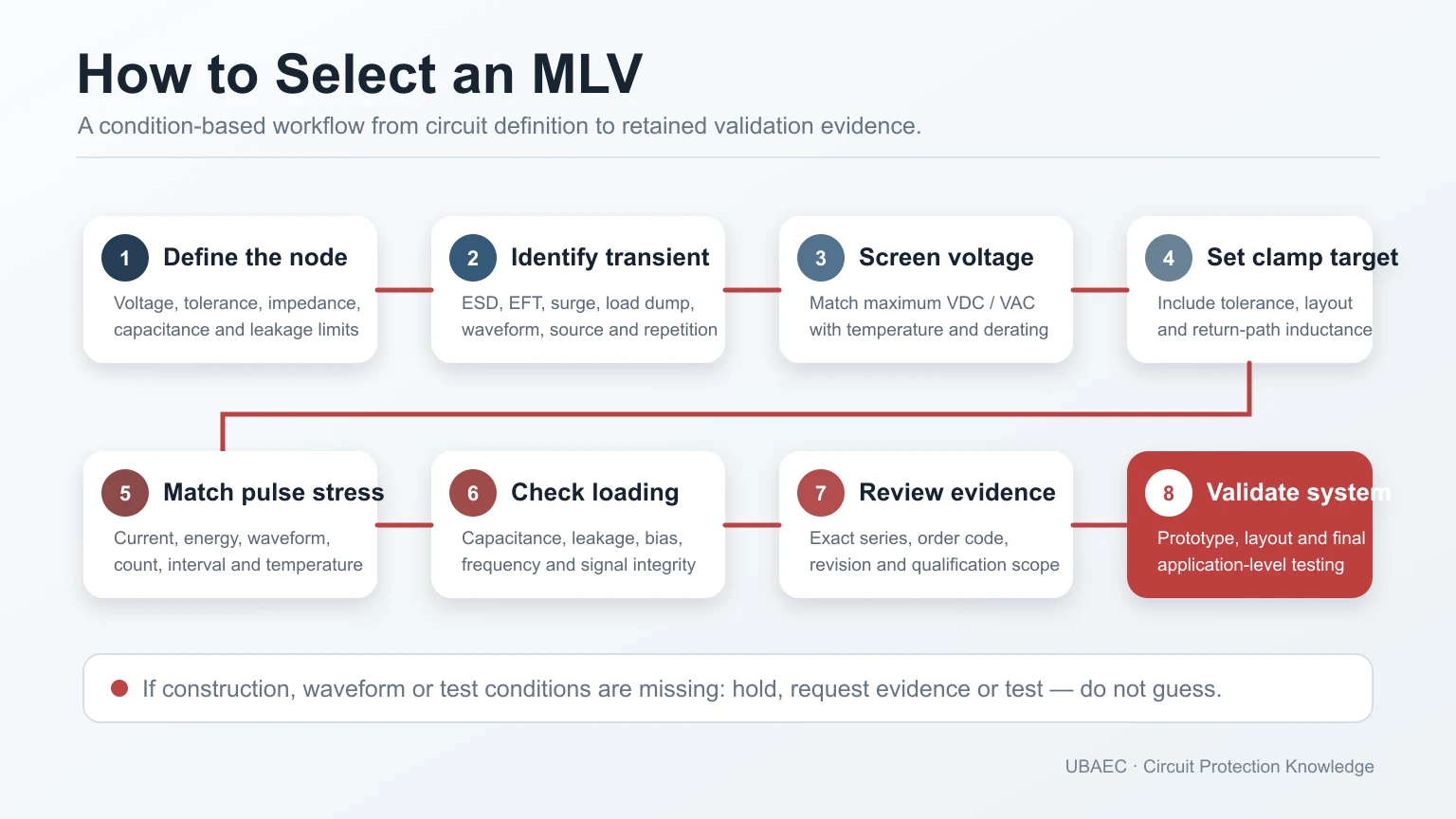
Selecting a multilayer varistor (MLV) is not a search for one nominal voltage or package size. It is a sequence that connects the protected circuit, transient source, allowed residual voltage, pulse conditions, signal loading, environment, layout and evidence for an exact current order code.
Use family pages for discovery; use the exact datasheet and final system test for selection.
Step 1 — Define the Node Before Looking at Parts
Record what is being protected and where the suppressor would connect:
- power rail, ground-referenced signal, differential line or exposed connector;
- normal DC and any AC/RMS component;
- supply tolerance, charging, ripple and temporary overvoltage;
- source and load impedance;
- maximum voltage the downstream device can tolerate;
- acceptable capacitance and leakage;
- intended transient-current return path.
Without these inputs, a part number may look plausible but cannot be validated.
Step 2 — Identify the Transient
Separate electrostatic discharge (ESD), electrical fast transient (EFT)/burst, switching spikes, 8/20 µs surge, 10/1000 µs or millisecond pulses, automotive transients and installation-level surge. Record waveform or generator, source impedance, peak level, polarity, event count, interval and temperature.
If the source is unknown, define a test plan or measurement task rather than selecting from an unrelated rating. A component’s Automotive Electronics Council AEC-Q200 status or International Electrotechnical Commission (IEC) reference does not replace the application transient definition.
Step 3 — Set the Continuous-Voltage Constraint
Screen candidates whose maximum continuous VDC—and VAC where applicable—covers the worst normal condition with the required derating. Do not use Vvar or Vc as the continuous-voltage limit. Consider abnormal-but-expected states that may last too long to be treated as a transient.
Step 4 — Define the Clamp Target
Start from the protected circuit’s voltage limit, not the MLV catalog. Build a budget for:
- MLV dynamic clamping at the expected current and waveform;
- part tolerance and temperature;
- trace, via and return-path inductive voltage;
- coupling paths that bypass the MLV;
- coordination with series impedance or other protection stages.
A datasheet Vc point at a different current does not prove the protected node will stay below its limit.
Step 5 — Match Pulse Current, Energy and Repetition
Compare the candidate’s pulse evidence with the real event. Keep Imax separate from the clamp-test current. Keep energy tied to waveform/duration. Check single-pulse, repetitive-pulse and lifetime or degradation limits separately.
For long automotive or mains-related events, require application-specific evidence and coordinated safety/failure controls. A short 8/20 µs rating does not prove load-dump or installation-surge suitability.
Step 6 — Check Capacitance, Leakage and Frequency Behavior
On power and slower control nodes, MLV capacitance may be acceptable or useful. On high-speed lines, screen it against the channel’s signal-integrity budget. Compare capacitance only at matched frequency, amplitude/bias, temperature and typical/maximum basis.
For arrays or filter structures, inspect the exact equivalent circuit and measured insertion-loss data. Do not predict full frequency response from capacitance alone. Leakage must be checked at the actual operating voltage and temperature, especially for battery-powered or high-impedance circuits.
Step 7 — Confirm Construction and Topology
Verify that the candidate is a construction-confirmed MLV rather than a molded SMD MOV, resin/polymer suppressor or ambiguous “SMD varistor.” For arrays, confirm element count, pinout, shared terminals and per-line versus package ratings.
Use the MLV terminology and product-boundaries guide before comparing adjacent technologies.
Step 8 — Check Package, Temperature and Assembly
Confirm dimensions, land pattern, termination finish, soldering process, operating/storage temperature, derating, board-flex risk and inspection needs. A larger package may offer a different pulse class, but package size alone is not an electrical cross-reference.
Use the MLV layout, mounting and soldering guide for current-path and ceramic-mechanical controls.
Step 9 — Verify Qualification, Revision and Lifecycle
Match qualification to the exact order code, revision and temperature scope. Recheck that the series and datasheet are current in the intended region. A family marketing page, old distributor record or archived PDF may help discovery but cannot establish current supply or qualification.
The reliability, standards and failure-modes guide separates component specification, qualification, equipment immunity and mission-profile evidence.
Step 10 — Compare Candidates in a Discrepancy Log
| Field | Candidate A | Candidate B | Decision |
|---|---|---|---|
| Construction and topology | Exact evidence | Exact evidence | Match / hold |
| VDC/VAC and derating | Value + conditions | Value + conditions | Pass / fail |
| Vvar | Range + test current | Range + test current | Comparable / mismatch |
| Vc | Voltage + current + waveform | Voltage + current + waveform | Comparable / test needed |
| Imax/energy/repetition | Original conditions | Original conditions | Pass / unresolved |
| Capacitance/leakage | Conditions + basis | Conditions + basis | Signal/power fit |
| Temperature/qualification | Exact scope | Exact scope | Pass / gap |
| Revision/lifecycle | Current evidence date | Current evidence date | Available / confirm |
Do not fill a missing value with zero, a family maximum or another package’s number. Mark it unresolved and request supplier confirmation or measurement.
Step 11 — Design the PCB Protection Path
Place the shunt device near the exposure point, minimize the loop and define where transient current returns on the printed circuit board (PCB). Check coordination with series impedance, filters, transient-voltage-suppression (TVS) diodes, primary surge devices or fusing where used. The system topology can be as important as the selected MLV curve.
Step 12 — Validate the Actual System
Test the chosen order code on the representative PCB with the required generator, coupling method, polarity, severity, sequence, temperature and acceptance criteria. Monitor the protected node and, when relevant, leakage, capacitance or Vvar before and after repeated stress.
A component rating or qualification does not establish equipment, module or vehicle compliance. Keep the final test report, PCB revision, device lot/order code and acceptance result with the design record.
Fast Reject Conditions
- continuous voltage is too low or unspecified;
- Vc is quoted without current/waveform or exceeds the clamp budget;
- pulse evidence uses an unrelated waveform;
- capacitance or leakage is incompatible with the node;
- construction or array topology is unresolved;
- temperature, qualification, lifecycle or assembly scope is missing;
- the recommendation depends on a family maximum rather than an exact order code.
Summary
A safe MLV selection moves from system inputs to exact, condition-matched product evidence and then to PCB/system validation. It does not start from a package photo or a single nominal voltage.
Continue Reading
- MLV Datasheet Parameters and Test Conditions
- MLV PCB Layout, Mounting and Soldering
- MLV Reliability, Standards and Failure Modes
- UBAEC Applications
Official Technical References
The following first-party, standards-organization or publisher records support the technical boundaries used in this article. Always verify the current revision and the exact product scope before design release.
- Voltage Protection Devices Product Map
- IEC 61000-4-2:2025 – Electromagnetic compatibility (EMC) – Part 4-2: Testing and measurement techniques – Electrostatic discharge immunity test
- Safety precautions for chip-type multilayer varistors
- Technical Support Tools for Chip Varistors / CTVS
- PCB Layout for ESD Countermeasures: ESD Visualization