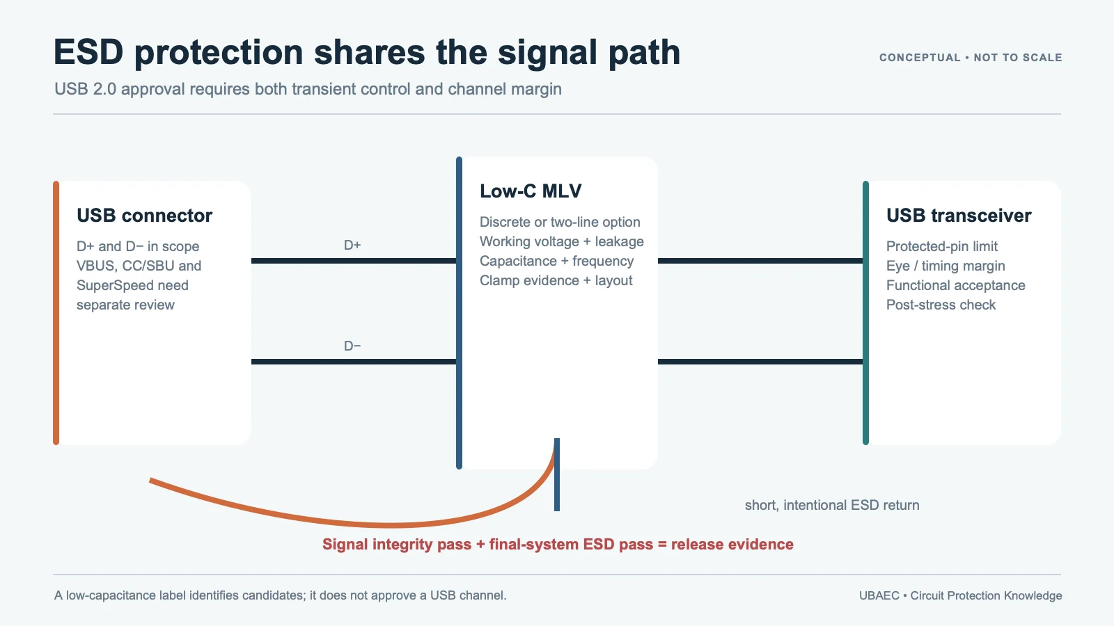
A USB connector is an ESD entry point, but adding a shunt device can also load the data pair. A suitable USB 2.0 protection design must divert the discharge before it reaches the transceiver while keeping D+ and D− within the signal-integrity budget.
A low-capacitance MLV can be a USB 2.0 protection candidate; the label alone does not approve it. The exact order code, PCB placement, return path and final product must satisfy both communication and ESD requirements.
Lock the USB Scope and Every Pin
First identify the connector and functions present. USB 2.0 uses D+ and D− for data, but the same connector may also expose VBUS, shield, identification, CC, SBU or SuperSpeed contacts. USB Type-C is a connector system, not proof that every pin has the same voltage, bandwidth or protection requirement.
This page covers USB 2.0 data-line ESD protection. It does not transfer a USB 2.0 MLV recommendation to USB 3.x, USB4, HDMI, DisplayPort, CC/SBU or power-delivery rails. The high-speed port protection guide owns those tighter-bandwidth technology trade-offs.
Define the ESD Event and Protected Node
Record the applicable IEC 61000-4-2 or customer test level, contact/air method, polarity, discharge point, generator network, shot count, operating state and functional acceptance. Decide where voltage must be limited: connector pad, protection-device pad or transceiver pin.
An MLV datasheet may list IEC 61000-4-2 capability, an 8/20 µs clamping voltage or a response-time statement. These are different evidence types. A component test does not prove the assembled product, and surge Vc does not equal the dynamic ESD voltage at the IC. See the MLV reliability and standards guide.
Select the Electrical Window
| Field | USB 2.0 design question | Release hold |
|---|---|---|
| Continuous voltage | Does VDC cover every valid D+/D− bias, tolerance and powered/unpowered state? | Only nominal signal level was checked |
| Leakage | Will guaranteed leakage preserve bias, detection and standby behavior across temperature? | Only a room-temperature typical value is available |
| Capacitance | Does maximum per-line loading fit the channel, including tolerance, frequency, bias and PCB parasitics? | Nominal or unmatched-frequency data is used |
| Varistor voltage | What min/nom/max range applies, and at what test current? | Vvar is treated as working or clamp voltage |
| Surge clamp | What Vc occurs at the stated current and waveform? | Values measured at different currents are compared |
| ESD response | What generator, fixture, node and measurement bandwidth support the result? | A static voltage rating is used as dynamic-clamp proof |
Use the MLV parameter and test-condition guide to translate the data. Current first-party examples show why conditions matter: Eaton’s MLVB table measures capacitance at zero bias, 1 Vrms and 1 MHz, while its starred low-capacitance clamp values use a different pulse current than the remaining entries. Do not remove those footnotes.
Low Capacitance Is a Trade-Off, Not a Winner Label
Lower capacitance generally reduces shunt loading, but it does not automatically provide the lowest protected-node voltage or the most pulse energy. In some MLV families, the very-low-capacitance options also have higher varistor and clamp voltages. The transceiver limit, event waveform and channel budget must be evaluated together.
Compare an MLV with a TVS/ESD diode array or another suppressor only at matched voltage, capacitance, waveform, temperature, package and layout conditions. The MLV versus TVS guide and MLV versus polymer/resin guide avoid universal technology claims.
Choose Discrete or Multi-Line Topology
Two discrete MLVs allow per-line placement and sourcing. An integrated two-line or array device may provide a supplier-defined relationship between elements and simplify routing. Confirm whether ratings are per element, per line, simultaneous or package-level and draw the internal circuit before approving the footprint.
For D+ and D−, account for capacitance mismatch as well as absolute loading. Package symmetry does not cancel unequal via, pad, trace and return-path parasitics.
Place the Protector in the ESD Current Path
Place the protection network close to the entry point in electrical-path terms: the discharge should encounter the protector and its intended return before a long branch reaches the transceiver. Keep the protected trace away from the high-current return path and minimize inductive loops.
The connector shield, chassis strategy, digital ground, enclosure and cable determine where current can flow. Do not route ESD through a narrow logic-ground trace simply because the MLV is physically near the connector. Review land pattern, solder process and board flex with the MLV layout and assembly guide.
Validate Signal Integrity with the Exact PCB
A capacitance number cannot capture the complete interconnect. Measure or simulate the exact MLV model, package, pads, vias and placement in the real channel. Use the method required by the product: eye diagram, TDR, insertion/return loss, edge timing, bit-error or functional margin.
Test multiple corners where relevant: minimum/maximum device capacitance, component tolerance, PCB revision, cable/connector, temperature and manufacturing variation. Passing on an evaluation board does not automatically pass the product enclosure and routing.
Validate the ESD Result at System Level
- Baseline: record USB enumeration, transfer behavior, signal margin, leakage and standby current.
- Dynamic measurement: observe the protected-node waveform with suitable bandwidth and a controlled probe/fixture.
- System ESD: test the final connector/enclosure points, both polarities, required shot count and operating states.
- Functional monitoring: detect reset, disconnect, corrupted transfer, latch-up or permanent damage.
- Post-stress review: recheck leakage, varistor voltage, communication margin and physical condition.
- Traceability: retain MLV order code/lot, PCB revision, cable, firmware, equipment and setup photographs.
Apply the engineering MLV selection workflow before freezing the BOM. If an alternate is introduced, repeat the evidence and PCB tests rather than assuming equal package and capacitance mean equal performance.
Minimum Inquiry Data
- USB connector type and every protected pin/function;
- USB 2.0 transceiver/SoC and protected-pin limits;
- data-line bias, powered/unpowered states and leakage budget;
- maximum allowed capacitance, balance and channel-loss budget;
- ESD standard, level, network, point, polarity, count and acceptance;
- schematic, layout, shield/ground path, cable and enclosure;
- temperature, package, lifecycle and production constraints.
Summary
USB 2.0 MLV protection requires a matched electrical and physical design: exact voltage/leakage, capacitance, clamp conditions, D+/D− balance, placement and return path. Approval comes only after signal-integrity and system-ESD validation on the final product.
Use the MLV Technical Resources & Datasheet Library, return to the MLV Knowledge Map, or ask UBAEC with the interface, schematic and test plan.
Continue Reading
- High-Speed Port ESD Protection: MLV, TVS and Low-Capacitance Trade-Offs
- MLV Datasheet Parameters and Test Conditions
- MLV PCB Layout, Mounting and Soldering Reliability
- MLV vs TVS Diode: How to Compare Protection Devices
Official Technical References
The following first-party, standards-organization or publisher records support the technical boundaries used in this article. Always verify the current revision and the exact product scope before design release.
- Multilayer varistors (MLVs) High-speed series datasheet
- MLVB low-capacitance multilayer varistor ESD suppressor datasheet
- Chip Varistor for ESD – SDV Series
- MLVG 0402 Series Specification A21
- Protecting High Speed Communication Ports
- IEC 61000-4-2:2025 – Electromagnetic compatibility (EMC) – Part 4-2: Testing and measurement techniques – Electrostatic discharge immunity test