

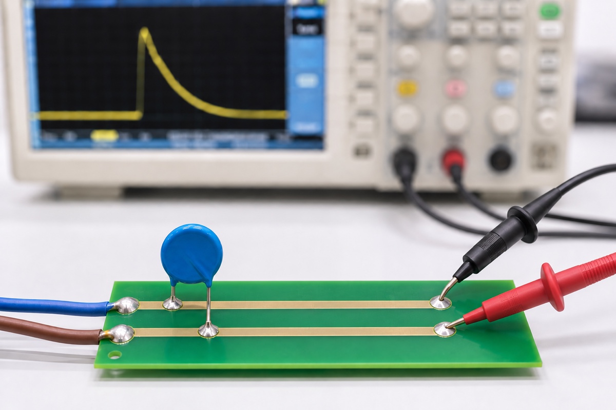
Why can the voltage at a protected circuit exceed the metal oxide varistor (MOV) clamping voltage in the datasheet? The two values describe different measurement boundaries. A datasheet value applies at a specified surge current, waveform, and component-terminal condition. The assembled-circuit voltage also includes parasitic impedance in leads, pads, PCB traces, vias, connectors, and the return path, plus any error introduced by the probing method.
The high-current loop matters more than the distance between symbols on a layout screen. When surge current changes rapidly, path inductance develops an additional voltage approximated by V=L·di/dt. If the same conductor carries both surge current and the protected load’s return, common impedance moves the load’s local reference as well. A healthy MOV can therefore coexist with excessive downstream stress.
Start by defining clamping voltage and residual voltage
Datasheet clamping voltage is normally measured at a stated peak current and pulse waveform, often 8/20 µs, and it includes the part’s specified tolerance. Different product families may use different test currents, so two parts with the same maximum continuous operating voltage (MCOV) cannot be compared from the clamping-voltage number alone. Current, waveform, initial temperature, pulse history, and terminal measurement boundary all belong with the value.
Residual voltage in a system is the transient voltage between two defined points. Voltage directly across the MOV, at the protected branch, at an IC supply pin, and between local circuit ground and chassis can all be different. A test report that states “650 V measured” without naming both probe points cannot distinguish a component problem from an interconnect, reference, or measurement problem.
Why tens of nanohenries can matter
Consider an illustrative 20 nH of added loop inductance. If surge current rises at 0.5 kA/µs, the idealized inductive contribution is about 10 V; at 2 kA/µs it is about 40 V. These numbers show scale only—they are not results for a particular PCB. Actual inductance depends on the geometry of both outgoing and return paths, while actual di/dt is shaped by generator impedance, MOV conduction, cabling, and the rest of the network.
The same relationship explains why “make the trace wider” is incomplete advice. More width lowers resistance and can reduce some inductance, but path length and loop area are often more influential. A short outgoing trace with a return that circles the board, or a topology that sends surge current through load ground before reaching the MOV, can still create a large shared-path voltage.
Use a system voltage budget to find the added stress
| Voltage contribution | Main dependencies | How to check it | Common mistake |
|---|---|---|---|
| MOV terminal voltage | part tolerance, surge current, waveform, temperature, history | differential measurement across the terminals with simultaneous current | comparing a remote-node peak directly with the datasheet |
| Entry-to-MOV path | length, loop area, vias, connector, di/dt | layout review plus parasitic estimate or extraction | judging proximity without tracing the return |
| MOV return-path voltage | chassis, protective-earth, and signal-return architecture | draw the complete surge-current loop | assuming every ground symbol is equipotential |
| Downstream ringing and probe error | network L/C, probe loop, bandwidth, common-mode range | change the probing method and compare full waveforms | treating induced pickup as device stress |
The entries are not guaranteed to add as scalar peaks because the surge network is dynamic and the waveforms may not reach their extrema at the same time. The table is a diagnostic framework. Capture MOV terminal voltage, downstream voltage, and surge current on the same timebase, then identify which path changes with the observed excess.
Route surge current around the sensitive circuit
Current entering from the connector should reach the suppression branch first and return through a short, wide, continuous path to the intended reference. The protected circuit should branch from the quieter side of that clamping point, creating a deliberate current split rather than sharing the surge conductor. An MOV can sit beside the connector yet remain ineffective if its return travels through a narrow digital-ground trace.
Keep both MOV leads short and avoid narrow copper necks between pads and the high-current path. When a layer transition is unavoidable, well-placed parallel vias can lower path impedance, but they must be close to the current entry and connect into a continuous return structure. Chassis, protective earth, and signal return should be joined only according to the system’s insulation, electromagnetic compatibility (EMC), and safety design.
Do not share a long conductor between surge current and a sense ground, controller ground, communications reference, or quiet analog return. Both L·di/dt and I·R across that common segment move the local reference. The MOV may clamp correctly to chassis while an IC pin experiences an excessive differential voltage relative to its own ground. A layout review should therefore include current arrows, not only component coordinates.
The probe can create a spike that is not present at the node
A long ground lead on a passive oscilloscope probe forms a pickup loop. In a high-di/dt and high-dv/dt field it can capture magnetic and electric interference and display a sharp spike that is not the intended node voltage. Use a short ground spring where voltage permits, a suitable high-voltage differential probe, or a safety-reviewed coaxial connection, and keep the two measurement conductors close together.
Bandwidth also belongs in the result. Excessive bandwidth may emphasize narrow ringing and pickup, while an overly restrictive limit may hide a real peak. A differential probe still must meet maximum differential voltage, common-mode voltage, common-mode transient rejection, input impedance, isolation, and safety-category requirements. Measuring directly across the MOV terminals and measuring from a downstream supply pin to its local return are different tests.
Two voltage points and one current trace improve diagnosis
A practical method is to capture one differential voltage directly across the MOV, a second at the protected load, and the surge current at the same time. The difference between the voltage traces is not automatically pure inductive drop because resistance, capacitance, coupling, and channel delay also exist. It does reveal how much interconnect and shared return contribute during the same event.
Repeat the test after shortening the loop, moving the branch point, or changing the return structure. If the downstream excess falls while MOV terminal voltage and current remain comparable, the evidence points to layout rather than a different MOV rating. Document changed geometry and probe connections so the result is reproducible.
Do not reduce acceptance to the first narrow spike. A protected IC may have separate limits for absolute peak voltage, pulse duration, injected clamp current, absorbed energy, reset, or functional upset. Compare the complete waveform with both component limits and the system immunity requirement.
A reviewable layout and validation procedure
- Draw the complete high-current loop from connector to suppressor to return on both the schematic and PCB, marking every segment shared with the load.
- Lock the exact MOV ordering code and record the datasheet clamping current, waveform, maximum or typical status, temperature, and tolerance.
- Shorten the device leads and both sides of the loop. Inspect pad neck-downs, vias, connectors, plane slots, and the location of the current split.
- Define three measurement boundaries: MOV terminals, the clamped branch, and the most sensitive downstream port, each with an explicit reference point.
- Select probes that meet differential, common-mode, bandwidth, isolation, and safety requirements, then minimize the physical measurement loop.
- Capture voltage and current together over required surge level, waveform, polarity, pulse count, interval, component tolerance, and temperature.
Frequently asked questions
Will a wider PCB trace solve excessive residual voltage?
Width helps resistance and some inductance, but total length, outgoing-to-return spacing, return location, vias, and shared impedance remain important. Close and shorten the loop before relying on added copper alone.
If an MOV responds quickly, why does layout still matter?
Fast material response does not remove L·di/dt voltage from the external conductors or keep remote reference points equipotential. System clamping is determined by the MOV and the entire current path.
Does a downstream peak above the datasheet value prove that the MOV is defective?
No. First align surge current, waveform, temperature, tolerance, measurement points, and probe method. A datasheet comparison becomes meaningful only after component-terminal voltage is separated from the added interconnect voltage.
Can simulation replace a surge test?
Simulation is useful for ranking loop and parasitic sensitivities, but models do not capture every assembly, cable, generator, and device variation. A representative system still requires controlled voltage-and-current validation under the applicable safety procedure.
Practical conclusion
MOV clamping voltage is a component-terminal result; downstream residual voltage is a system-node result. Parasitic inductance, shared return, network ringing, and probing method create the difference. The useful layout rule is more precise than “place the MOV close”: give surge current the smallest closed loop that bypasses sensitive conductors, then verify MOV voltage, downstream voltage, and current at explicit measurement boundaries.
Continue with MOV Protection Circuit Basics, MOV Clamping Voltage, MOV Surge Waveforms, and MLV Layout, Mounting and Soldering.







Comments 1