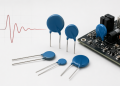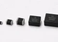
An audio jack, microphone line, antenna feed and RF control node may all be exposed to user or connector ESD, but they impose different electrical limits. Audio circuits are judged by frequency response, noise, distortion and audible artifacts. An antenna path is judged by matching, insertion loss, return loss, sensitivity or transmitted power over an exact band.
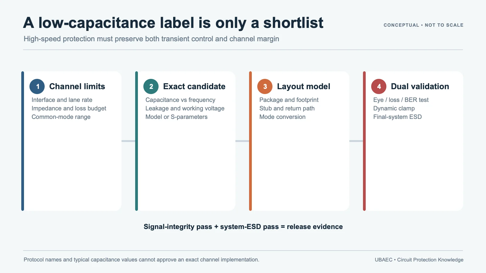
“Low capacitance” is a screening label, not proof of RF compatibility. An MLV is only one candidate. The exact part, topology, bias, PCB, matching network and final enclosure must pass both signal-performance and ESD tests.
Classify the Node Before Selecting a Protector
| Node | Loading concern | Performance evidence |
|---|---|---|
| Analog audio input/output | Leakage, nonlinear capacitance, source/load impedance and bias | Frequency response, THD+N, noise, click/pop and functional ESD |
| Microphone or sensor audio | Low signal level, bias supply, noise and controller clamp | Sensitivity, noise floor, distortion and recovery after ESD |
| Antenna feed | Added capacitance/inductance, pad discontinuity and matching shift | S11/return loss, tuning, efficiency or sensitivity across the exact band |
| RF-adjacent control/data | Bandwidth, common-mode range, leakage and coupling | S21/insertion loss, waveform/link result and operating-state ESD |
Start with the parameter and test-condition guide. Capacitance needs an exact order code, tolerance, frequency, measurement amplitude, DC bias and typical/maximum basis. A single nominal pF value cannot predict a circuit’s full frequency response.
What Current Manufacturer Evidence Supports
KYOCERA AVX’s current ASPGuard document describes low-capacitance varistors for RF circuits, sensors, antennas, data lines and radar. It lists exact parts, working voltage, capacitance and tolerance, clamp conditions, energy and 8/20 µs peak current, and includes S21 examples. Those plots support evaluation of the named devices; they are not generic performance for every PCB, matching network or frequency band.
TDK’s current hosted high-speed-series document covers discrete and array constructions and preserves part-specific capacitance and electrical conditions. Its front-page withdrawal notice names two order codes; do not generalize that notice to the entire document, but confirm lifecycle for every exact code before selection. Panasonic’s technical page shows chip-varistor use on audio lines while distinguishing extremely low-capacitance polymer ESD suppressors for antenna and high-speed paths. AMOTECH’s mobile application page adds placement discovery. Together they justify comparison, not a universal MLV recommendation.
Follow the MLV selection workflow and use the high-speed port protection method only for its evidence discipline. Audio and antenna circuits still need their own acceptance criteria.
Evaluate the Entire RF Discontinuity
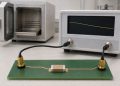
At RF, the package, pads, via, ground path and nearby matching components can matter as much as nominal capacitance. Simulate or measure the protector in the intended shunt position. Record the reference impedance, fixture/de-embedding method, frequency span, bias and PCB stack-up. Review S11 or return loss, S21 or insertion loss, tuning shift and the application metric that matters to the radio.
For an automotive antenna or Ethernet-adjacent node, the automotive Ethernet and RF-adjacent guide adds qualification and harness context. It does not transfer an automotive order code to a consumer or telecom RF circuit.
Evaluate Audio as Audio
On an analog audio path, verify that protector leakage and nonlinear capacitance do not introduce bias error, frequency-response change, harmonic distortion or noise. Test muted, active, plug/unplug and powered-off states. A device can pass an audio sweep but still cause an audible click, controller reset or temporary mute during ESD.
Compare technologies with the MLV versus TVS diode and MLV versus polymer ESD suppressor guides. Clamp behavior, capacitance, leakage, endurance, failure response and availability must be reviewed together; no technology wins every audio or RF node.
Control Placement and the Return Path
Place the candidate so the ESD current reaches the intended chassis or local return before it crosses the protected circuit. TDK’s controlled board experiment showed a meaningful difference between approximately 10 mm and 40 mm placements, but those distances belong to that board and test. They are not an antenna-layout rule.
Review connector shield, enclosure seam, ground impedance, via placement and routing with the layout, mounting and soldering guide. If an array or feedthrough device is considered, retain channel topology, matching and crosstalk using MLV arrays and feedthrough filters.
Final Validation Flow
- Measure baseline audio or RF performance on the final connector, matching network, PCB and enclosure.
- Add the exact protector and repeat frequency, noise, distortion, S11/S21 and application-level measurements.
- Run documented contact, air and indirect ESD at realistic entry points and operating states.
- Observe residual voltage, current route, resets, audible artifacts, link/image/radio behavior and recovery.
- Recheck leakage, capacitance-sensitive performance and physical condition after repeated strikes.
- Repeat after any order-code, pad, via, shield, matching component, enclosure or PCB change.
Minimum Inquiry Data
- node type, connector, audio function or RF band, impedance and operating states;
- protected IC/module limits, normal voltage, bias, source/load impedance and matching/filter network;
- maximum acceptable capacitance and leakage with frequency, amplitude, bias, tolerance and typical/maximum basis;
- required S-parameter, frequency-response, noise, distortion, sensitivity or transmitted-power acceptance;
- ESD generator, contact/air point, polarity, shot count, return path, package, lifecycle and enclosure/PCB revision.
Summary
Audio and RF-adjacent protection is released by measured circuit performance plus final-system ESD behavior. Low capacitance identifies candidates; it does not replace band-, impedance-, noise- and layout-specific evidence.
Consult the MLV Technical Resources & Datasheet Library or return to the MLV Knowledge Map.
Continue Reading
- High-Speed Port ESD Protection: MLV, TVS and Low-Capacitance Trade-Offs
- MLV vs Resin and Polymer ESD Suppressors
- MLV PCB Layout, Mounting and Soldering Reliability
- How to Select an MLV: A Practical Engineering Workflow
Official Technical References
The following first-party, standards-organization or publisher records support the technical boundaries used in this article. Always verify the current revision and the exact product scope before design release.