Reverse working maximum voltage (VRWM), breakdown voltage (VBR), and clamping voltage (VC) are all expressed in volts on a TVS diode datasheet, but they are not three names for the same limit. They identify different operating points on the current-voltage characteristic: continuous reverse operation, breakdown at a specified small test current, and the device voltage at a specified large pulse current.
Using only one of these numbers creates two common errors. VBR may be mistaken for the highest normal line voltage, or it may be treated as the voltage that the protected load will see during a surge. A defensible selection first closes the normal operating window, then maps the actual transient current to a maximum clamping voltage, and finally adds the voltage contributed by package and PCB inductance at the relevant measurement point.
Read each voltage with its current condition
| Parameter | Datasheet operating point | Question it answers | What it cannot replace |
|---|---|---|---|
| VRWM | Reverse leakage region, usually with IR specified | Maximum continuous reverse working voltage | It does not define avalanche onset or high-current clamping |
| VBR | Specified DC test current IT; often a minimum or a range | Small-current breakdown reference and tolerance band | It is neither a continuous rating nor VC |
| VC | Specified peak pulse current IPP and waveform | Maximum device voltage at that pulse condition | It cannot be compared without IPP, waveform, and temperature |
The word “maximum” also applies to different things in the three rows. VRWM is a working-region boundary, VBR may have minimum and maximum production limits, and VC is commonly a maximum at a defined IPP and waveform. Before comparing two series, align the test current, pulse shape, initial junction temperature, and maximum-versus-typical status. A lower-looking voltage from a different test condition is not automatically a better clamp.
VRWM protects the normal operating window
VRWM, also called reverse standoff voltage, is the reverse voltage that may be applied continuously under stated conditions while the TVS remains in its low-leakage region. The design input is not merely the nominal rail. It includes supply tolerance, steady ripple, charger or regulator high-side error, ground shift, and any credible long-duration abnormal state that the circuit is expected to tolerate.
The highest sustained voltage should remain below VRWM, but that inequality alone does not prove adequate margin. Reverse leakage current IR is normally specified at VRWM and can change substantially with temperature. Leakage may matter in high-impedance nodes, battery equipment, and low-power standby modes. On AC, differential, or polarity-reversing lines, define the voltage and reference in both directions before applying a unidirectional or bidirectional rating.
VBR is a reference point at test current IT
VBR is tied to a stated test current IT. A manufacturer may specify it at 1 mA or another current and may publish a minimum, a range, or both; the exact condition belongs to the selected series. This point defines avalanche behavior and production tolerance. It does not mean that current is exactly zero below VBR, nor does it mean voltage stops rising after breakdown begins.
VBR therefore cannot replace VRWM. Operating a line near VBR can produce unintended leakage, heating, or early conduction during normal variation. VBR also cannot replace VC because surge current is usually far above IT. The TVS dynamic resistance causes its terminal voltage to rise as pulse current increases. If a datasheet gives only a minimum VBR, the designer must not invent a typical value or upper bound.
VC belongs to an IPP, waveform, and temperature
Clamping voltage VC is the measured or guaranteed device voltage at a specified peak pulse current IPP and waveform. A statement such as “VC is 20 V” is incomplete unless the associated current and pulse condition are preserved. Pulse duration and shape affect current capability, junction heating, and response. Repetitive exposure adds duty cycle, interval, and thermal recovery conditions that a single-pulse row does not cover.
The application does not automatically drive the datasheet’s maximum IPP. Actual current is established jointly by the transient source voltage, source impedance, added series impedance, protected circuit, and nonlinear TVS characteristic. Solve or measure that operating point, then use the maximum VC or the applicable clamping curve from the same series. The power number in a family name is not a substitute for this load-line calculation.
Dynamic resistance explains a trend, not a new rating
Between two nearby pulse-current points, dividing the voltage change by the current change gives an incremental dynamic-resistance estimate. It helps explain why VC rises above the small-current breakdown region as IPP increases. The slope is only an approximation over that current interval, waveform, and junction-temperature range. It should not be extrapolated to zero current, another pulse width, or another package.
Some advanced TVS structures use snapback or other low-clamping behavior, so their current-voltage shape differs from that of a conventional avalanche TVS. A single “VBR plus current times resistance” expression is especially unsafe across those transitions. Trigger, holding, clamping, and recovery conditions must instead be taken from the specific manufacturer’s document.
Device VC is not always the load residual voltage
Datasheet VC describes voltage across the TVS under its specified setup. On a PCB, traces and vias between the port, TVS, return, and protected load have parasitic inductance. A fast current change produces an additional L·di/dt term. A probe connected at the load may therefore read more voltage than a probe placed directly across the TVS terminals; the two measurements include different portions of the current path.
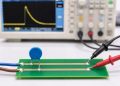
Validation should use a short diversion path, a defined local return, and a probing method with appropriate bandwidth and loop area. Record the generator waveform, source impedance, probe location, and grounding method. The system acceptance limit should compare the worst residual voltage at the protected node with the downstream device’s withstand for the same polarity and duration, rather than comparing two isolated headline ratings.
A six-step TVS voltage-window check
- List the highest sustained line voltage, including tolerance, ripple, offset, reverse connection, and credible steady faults.
- Select VRWM and check IR, standby power, and signal bias at the highest relevant temperature.
- Read the complete VBR range and IT so normal variation does not enter an unwanted avalanche region.
- Calculate or measure actual IPP from the specified transient source and impedance while retaining pulse width, waveform, polarity, and repetition.
- Use maximum VC at the applicable condition, then add package, layout, and return-path residual voltage.
- Close peak power, energy, temperature derating, repetitive-pulse, package thermal, and downstream-withstand checks independently.
Application constraints remain important after these six steps. High-speed data lines add capacitance and signal-integrity limits. Automotive power lines require the applicable pulse standard and source impedance. AC and differential interfaces require explicit unidirectional-versus-bidirectional behavior. Two devices with equal VRWM are not interchangeable when their VBR tolerance, VC at IPP, leakage, capacitance, package, or qualification differs.
FAQ
Can VBR be used as clamping voltage?
No. VBR is defined at the relatively small test current IT; VC belongs to a specified large pulse current IPP. They are different operating points, and surge voltage must retain the actual IPP, waveform, and temperature condition.
Does a VRWM closer to the normal rail always protect better?
No. A lower VRWM may reduce part of the protection window, but it may also increase leakage or cause conduction during normal tolerance, ripple, or high temperature. Selection must satisfy both non-operation in normal use and acceptable residual voltage during the transient.
Are TVS diodes with the same VRWM interchangeable?
Not from VRWM alone. Compare the VBR range and IT, maximum VC and IPP/waveform, pulse-power derating, leakage, capacitance, polarity, package, qualification, and the result of the intended system test.
Practical conclusion
VRWM, VBR, and VC are different boundaries of one protection window. VRWM governs continuous normal operation, VBR defines a small-current avalanche reference, and VC states a clamping result at a specified large pulse condition. Read every value with its current, waveform, temperature, and maximum-or-typical status. After the device check, include source impedance, PCB parasitics, and protected-node measurement before accepting a TVS selection or substitution.
Continue with MLV vs TVS Diode, MOV vs TVS Diode, Datasheet Parameters and Test Conditions, and the UBAEC contact page.