Touch panels, mechanical keys and camera connectors are all exposed to people, cables or enclosure openings, but they are not one electrical interface. A mechanical button may tolerate substantial shunt capacitance. A capacitive touch electrode can be sensitive to leakage and added capacitance. A camera data lane may require controlled impedance and broadband signal-integrity evidence.
Do not choose one “low-capacitance MLV” for all three by label alone. Define the entry point, signal or rail, return path, controller limits and final ESD test before selecting an MLV, TVS array, polymer suppressor or coordinated combination.
Classify the Exposed Interface
| Interface | Primary electrical constraint | Required validation |
|---|---|---|
| Mechanical key or switch | Debounce network, pull-up/down, leakage and controller pin clamp | Direct/indirect ESD and stuck-key or false-trigger behavior |
| Capacitive touch electrode | Baseline capacitance, sensitivity, scan frequency, leakage and environmental drift | Touch performance before, during and after enclosure ESD |
| Camera or high-speed data | Impedance, bandwidth, pair/lane balance, insertion/return loss and receiver margin | Image/link performance with the exact flex, connector and PCB |
| Camera power/control | Rail tolerance, I/O state, clamp window and sequencing | Functional ESD, latch-up, reset and post-stress leakage |
Use the parameter and test-condition guide. Capacitance needs frequency, amplitude, DC bias, tolerance and typical/maximum basis. Leakage needs applied voltage and temperature. ESD performance needs the network, polarity, contact or air method, pulse count and functional criterion.
Use Application Pages as Placement Evidence
AMOTECH’s mobile-phone application page and Thinking’s appliance guides identify keypad, interface, display and touch-panel positions where suppressors may be used. Thinking also separates an input MOV from a TVM-G ESD suppressor at the display/touch area. These diagrams are useful for discovery and architecture discussion; they do not provide an exact capacitance budget, dynamic clamp curve or final-system approval.
A supplier family application list is therefore the start of the MLV selection workflow, not its conclusion. Obtain the current order-code datasheet and lifecycle state, then verify the actual electrical node.
Lifecycle Is a Release Gate
Bourns’ current CGA-MLA document lists cameras, sensors, touch screens, HDMI and other interfaces, but it also states that the series is available and not recommended for new designs. UBAEC should not recommend CGA-MLA for a new design. The named BVRA0603, BVRA0805 and BVRA1206 families are leads for independent review, not automatic drop-in replacements.
An alternate must match working voltage, leakage, varistor or breakdown range, dynamic clamp, capacitance conditions and tolerance, package/land pattern, temperature, pulse endurance and lifecycle. Use the reliability and standards guide.
Placement Means Controlling the Current Path
TDK used an ESD visualization system to compare a chip varistor mounted approximately 10 mm and 40 mm from the injection point on a stated board. Under that controlled setup, the closer location diverted current earlier and improved the LED result. The useful principle is to identify the intrusion route and create a short, low-impedance shunt path near the entry point.
The two distances are not a universal design rule. Enclosure seams, flex cables, ground geometry, vias, connector shields and the impedance of the intended return can change the current route. A protector placed “near” the connector can still fail if its return trace forces the pulse through the controller. Apply the layout, mounting and soldering guide on the final PCB.
Control Loading by Interface
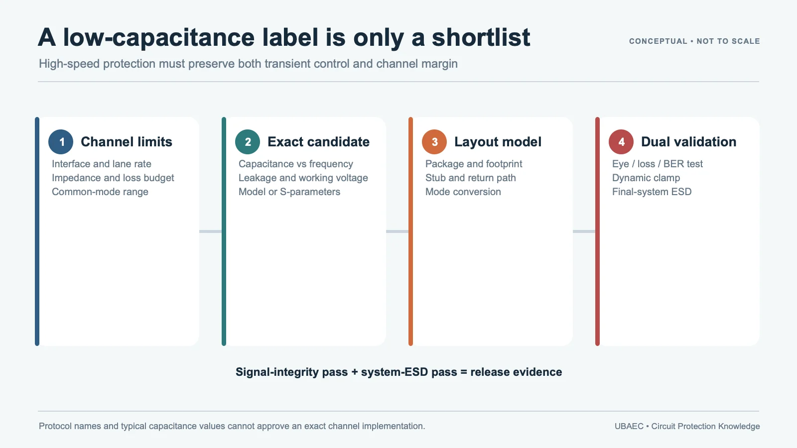
For a mechanical key, confirm that leakage cannot change logic state and capacitance does not impair debounce or scanning. For capacitive touch, measure baseline shift, sensitivity, wet/glove behavior and drift across voltage and temperature. For camera data or another broadband line, nominal capacitance alone is inadequate; require the exact device’s S-parameters or measured insertion/return loss and image/link margin.
Use the high-speed port protection method for camera data and the USB 2.0 ESD guide only as methodology. Neither creates a camera-specific capacitance limit. Compare MLV and diode behavior in the MLV versus TVS diode comparison.
Multiple keys or lanes may suggest an array or feedthrough structure, but channel matching, common electrode/ground architecture, crosstalk and fault behavior must fit. See MLV arrays and feedthrough filters.
Final Enclosure ESD Validation
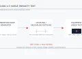
- Map direct contact, air-discharge and indirect-coupling points on the actual enclosure.
- Document the IEC 61000-4-2 network or other method, polarity, levels, pulse count, interval and functional criterion.
- Measure the current path and residual voltage at the protector and controller where practical.
- Exercise every key, touch zone, camera mode, cable state and power sequence during testing.
- Check false touches, missed inputs, image errors, resets, latch-up, leakage and parameter drift after stress.
- Repeat with production enclosure materials, flex cables, connectors, PCB revision, firmware and component alternates.
Component claims and supplier demonstrations do not establish equipment immunity. Release depends on the actual enclosure, user contact path, cable, board and operating state.
Minimum Inquiry Data
- interface type, voltage, impedance, scan or data rate and controller limits;
- capacitance/leakage budget with measurement conditions and tolerance;
- enclosure, connector, flex, shield/ground and intended transient return;
- ESD network, contact/air/indirect points, pulse count and acceptance criterion;
- exact order code, lifecycle, package, temperature and final test plan.
Summary
Touch, keypad and camera protection starts with interface classification. An MLV is released only when its loading, clamp behavior, placement, lifecycle and final-enclosure ESD result fit that exact interface.
Consult the MLV Technical Resources & Datasheet Library or return to the MLV Knowledge Map.
Continue Reading
- USB 2.0 ESD Protection with Low-Capacitance MLVs
- High-Speed Port ESD Protection: MLV, TVS and Low-Capacitance Trade-Offs
- MLV PCB Layout, Mounting and Soldering Reliability
- How to Select an MLV: A Practical Engineering Workflow
Official Technical References
The following first-party, standards-organization or publisher records support the technical boundaries used in this article. Always verify the current revision and the exact product scope before design release.