LIN and CXPI are single-line automotive communication interfaces. Their protection problem is different from a differential CAN pair: the designer must preserve the line’s dominant and recessive behavior while handling connector ESD, harness-coupled transients and abnormal vehicle-voltage conditions.
An automotive MLV is a candidate shunt protector only when its continuous voltage, leakage, clamp behavior, pulse capability and capacitance fit the exact interface. A family application label is not an order-code recommendation, and the completed ECU or module still requires the applicable automotive tests.
Define the Interface Before Selecting the MLV
Record whether the design is LIN or CXPI, the transceiver order code, supply architecture, bus pull-up or bias network, normal line levels, voltage tolerance, current limits and protected-pin absolute maximums. Include powered, unpowered, sleep, wake and fault states if they are part of the module requirement.
Do not find LIN evidence by matching the letters inside “multilayer.” LIN must appear as a standalone application term in a current first-party source. Current TDK, KYOCERA AVX and Eaton material identifies LIN-family use, but each source still points to a family or set of exact models with its own ratings.
Separate the Transient Problems
| Stress | Information required | What cannot be inferred |
|---|---|---|
| Connector/harness ESD | Generator network, contact/air method, polarity, point, discharge count, module state and protected-node waveform | System ESD immunity from an MLV voltage rating |
| Coupled signal-line transient | Coupling method, harness, level, source impedance, duration, repetition and operating mode | ISO 7637-3 performance from a generic 8/20 µs current value |
| Supply or long-pulse disturbance coupled into the interface | Vehicle network, rail condition, duration, energy path and coordination with upstream protection | Load-dump survival from an ESD test or a short surge rating |
| Normal communication | Dominant/recessive levels, edge timing, leakage, capacitance and temperature | Signal integrity from a “low-capacitance” label alone |
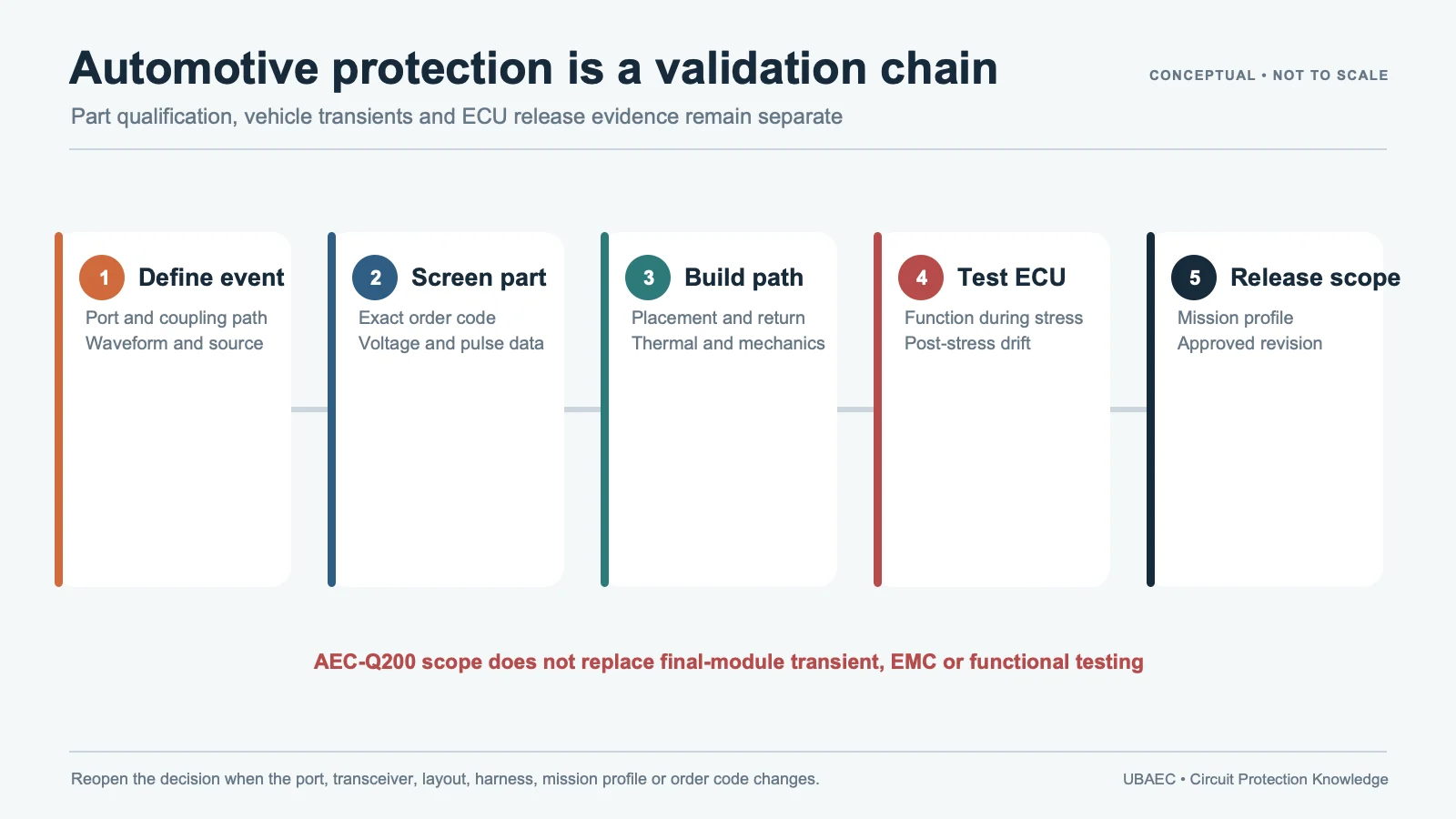
Keep the test object visible. IEC or ISO equipment/module immunity, AEC-Q200 passive-component qualification and a supplier’s part-level pulse test answer different questions. The MLV reliability and standards guide defines these layers.
Build the Protection Architecture
A typical design places a shunt suppressor near the exposed connector so transient current can return through a short, intentional path. A series resistor, coil or bead may be present for current limiting or noise control, and the transceiver may include internal protection. An upstream supply-line protection stage can be necessary when the interface may experience longer or higher-energy events.
These elements are coordinated; they are not interchangeable. The series element affects pulse current and communication edges. The MLV affects clamp voltage, leakage and shunt capacitance. The return path and reference choice determine where the transient current actually flows. The final values and ordering belong to the transceiver vendor guidance, EMC design and module test plan.
Use the MLV layout and assembly guide to review current path, land pattern, solder process and board flex. Do not publish or apply a universal placement distance.
Select Continuous Voltage and Leakage First
The MLV must remain in its high-resistance state throughout every valid bus condition. Compare its maximum continuous DC rating against the line’s normal range, supply tolerance, wake/sleep behavior, reverse or offset conditions and required temperature margin. Nominal battery voltage or nominal logic level alone is not enough.
Leakage is measured at a defined voltage and temperature. Excess leakage can shift the recessive level, load the bias network or increase standby current. Use a guaranteed limit where the design needs one; do not treat a room-temperature typical value as a worst-case specification.
Match Clamp Behavior to the Transceiver Limit
Varistor voltage, continuous voltage and clamping voltage are separate fields. A clamp value is meaningful only with the injected current, waveform and temperature. The voltage at the transceiver pin also includes interconnect inductance, source impedance, series elements and the return path.
Surge Vc measured with an 8/20 µs current pulse is not an ESD dynamic-clamp waveform. Likewise, peak current does not state the voltage that reaches the protected node. Translate each supplier table using the MLV parameter and test-condition guide.
Retain Pulse Duration, Energy and Repetition
Automotive signal lines may encounter coupled pulses whose source and duration differ greatly from a short component surge. Preserve the pulse generator or coupling method, source impedance, peak, duration, repetition, interval, temperature and pass criterion. An energy number without its waveform is incomplete.
If a long-duration event can reach the line, determine whether the local MLV is only a secondary clamp in a staged architecture. Review current limiting, upstream TVS/MOV protection, fusing or fault containment as applicable. The neighboring automotive local-rail protection guide owns supply-rail coordination rather than this signal-interface page.
Check Capacitance and Communication Behavior
LIN and CXPI do not use a matched differential pair, so inter-line balance is not the primary issue. The MLV’s capacitance and leakage still load the bus, interact with the pull-up/bias and series network, and can change edge timing or noise margin.
Retain capacitance frequency, amplitude, DC bias, temperature, tolerance and typical/maximum basis. A current TDK automotive catalog, for example, lists different exact parts for LIN/CXPI, Classical CAN and CAN/CAN-FD. That separation is a useful warning: do not transfer a CAN part or its capacitance target into a LIN/CXPI design without a new review.
Use Exact Automotive Evidence
AEC-Q200 wording must be tied to the exact order code, package, termination, temperature grade and supplier declaration. It does not establish protocol compliance or guarantee the ECU against ISO 10605, ISO 7637 or an OEM plan.
Use current manufacturer product pages or application guides to discover candidate families, then use the current exact datasheet or delivery specification for numeric decisions. Confirm lifecycle and revision before release. The engineering MLV selection workflow records the requirement and evidence trail.
Validation Plan for LIN or CXPI
- Static states: verify bus voltage, leakage and current in powered, unpowered, sleep, wake and defined fault conditions across temperature.
- Communication: measure dominant/recessive levels, rise/fall behavior, timing, error rate and wake behavior with the final harness loading.
- Protected-node clamp: measure at the transceiver pin under the specified pulse or ESD setup, not only at the connector or generator.
- Automotive immunity: run the applicable ISO 10605, ISO 7637-3 or OEM/customer test with exact polarity, repetition, operating mode and functional criterion.
- Thermal and degradation: record MLV temperature, leakage, varistor-voltage drift, clamp behavior and physical condition after repeated events.
- Production controls: retain MLV lot, PCB revision, placement, soldering, inspection and test-equipment configuration.
When a candidate part changes, use the MLV cross-reference method. Similar package size and nominal varistor voltage are not enough to approve an alternate.
Minimum Inquiry Data
- LIN or CXPI transceiver and module function;
- bus/supply voltage in all normal, sleep, wake and fault states;
- pull-up/bias, series resistor/coil/bead and connector/reference topology;
- protected-pin limit and maximum acceptable clamp voltage;
- ESD and transient networks, levels, duration, repetition and acceptance criteria;
- capacitance, leakage, timing and standby-current budgets;
- temperature, package, qualification, lifecycle and production requirements.
Summary
LIN and CXPI MLV protection starts with valid bus voltage and leakage, then clamp conditions, pulse duration, capacitance, qualification, topology and layout. It ends with dominant/recessive communication, ESD, coupled-transient and post-stress validation on the actual module.
Review the related CAN and CAN FD protection guide, use the MLV Technical Resources & Datasheet Library, return to the MLV Knowledge Map, or ask UBAEC with the transceiver, schematic and test requirements.
Continue Reading
- CAN and CAN FD Protection with Multi-Element MLVs
- MLV Arrays, Multi-Element Devices and Feedthrough Filters
- MLV Datasheet Parameters and Test Conditions
- MLV Reliability, Standards and Failure Modes
Official Technical References
The following first-party, standards-organization or publisher records support the technical boundaries used in this article. Always verify the current revision and the exact product scope before design release.
- Chip varistors: Automotive grade AVR series catalog
- Automotive Circuit Protection Application Guide
- AMLV automotive grade multilayer varistor datasheet
- Automotive EZJ-P multilayer SMD varistors
- ISO 7637-3:2016 – Road vehicles – Electrical disturbances from conduction and coupling – Part 3: Electrical transient transmission by capacitive and inductive coupling via lines other than supply lines
- ISO 10605:2023 – Road vehicles – Test methods for electrical disturbances from electrostatic discharge